Method for detecting offset position of wafer

A technology of offset position and wafer, which is applied to measurement devices, optical devices, complex mathematical operations, etc., can solve problems such as inability to proceed, wafer damage process, errors, etc., and achieve the effect of improving repeatability and avoiding wafer damage.

Active Publication Date: 2010-09-15
ADVANCED MICRO FAB EQUIP INC CHINA
View PDF4 Cites 12 Cited by
  • Summary
  • Abstract
  • Description
  • Claims
  • Application Information

AI Technical Summary

Problems solved by technology

[0012] Because in actual operation, the offset of the wafer in the X-axis direction and the Y-axis direction is sometimes very small, the measured data will produce errors, and then the measured value is substituted into the square root formula for calculation, which will inevitably introduce greater errors. The accurate offset value cannot be guaranteed, so the position of the wafer cannot be accurately corrected, and there are still consequences that cause damage to the wafer or failure of the process

Method used


Image

  • Method for detecting offset position of wafer
  • Method for detecting offset position of wafer
  • Method for detecting offset position of wafer

Examples


Embodiment Construction

[0100] The following evidence Figure 2-Figure 4 , specify the preferred embodiment of the present invention:

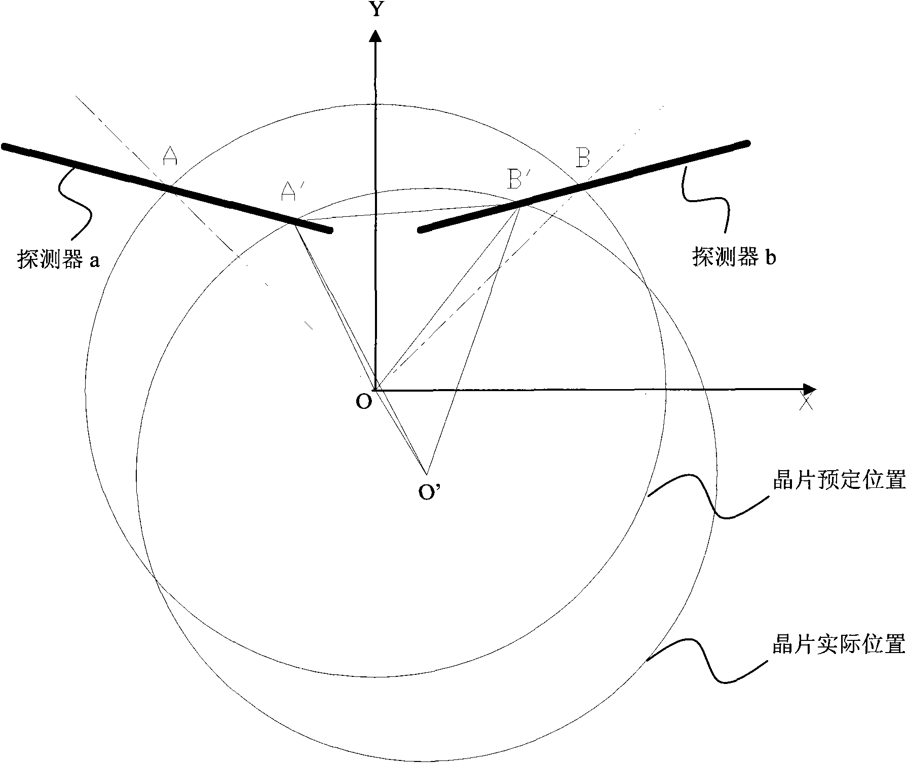
[0101] Such as figure 2 As shown, the center of the wafer at the predetermined position is O, and the center of the wafer after the offset is O'. Two detectors a and b are arranged around the wafer, and the detection direction of the detector is along the radial direction of the predetermined position of the wafer. Arrangement, there is no linear positional relationship between the two detectors, the two detection points on the edge of the wafer at the predetermined position detected by the detector are respectively A and B, and the two detection points on the edge of the wafer after the offset detected by the detector The detection points are A' and B' respectively;

[0102] For the setting of two detectors, the two-point method can be used for detection, and the detection method includes the following steps:

[0103] Step 2.1, the detector detects and obtains t...


PUM


Abstract

The invention discloses a method for detecting an offset position of a wafer by determining the offset of a central point of the wafer. The method comprises the following steps of: arranging a plurality of detectors around the wafer, arranging the detecting directions of the detectors along the radial direction of a predetermined position of the wafer, ensuring that any two detectors have no linear position relationship, and measuring and calculating the offset position of the wafer according to different numbers of the arranged detectors by selectively adopting a two-point method, a three-point method, a mean value two-point method or a mean value three-point method. The method improves the repeated precision of wafer transmission during manufacturing, and avoids wafer damage due to the offset of the wafer position.

Description

technical field [0001] The invention relates to the field of semiconductor manufacturing, in particular to a method for detecting the offset position of a wafer. Background technique [0002] In the manufacture of semiconductor integrated circuits, many processes are carried out in the wafer state. For the wafer, each process is completed in the corresponding process chamber. Wafer transfer mechanisms are used to move wafers between chambers, taking wafers out of one chamber and placing them in another chamber. During the movement of the wafer, it must be ensured that the wafer is placed precisely in the predetermined position in the process chamber. [0003] It is a common practice to use a manipulator as a wafer transfer mechanism. The manipulator includes several rotating arms, and the wafer is loaded on the wafer position of the rotating arm at the end of the manipulator. to predetermined locations in different process chambers. If the wafer is accurately loaded to th...

Claims


Application Information

Patent Timeline
Patent Type & Authority Applications(China)
IPC IPC(8): G01B11/02G06F17/10
Inventor 陶珩王伟娜朱玉东袁群艺
Owner ADVANCED MICRO FAB EQUIP INC CHINA
Why Eureka
Try Eureka