Method for Nandflash USB controller to read and write Norflash memory

A disk controller and memory technology, applied in read-only memory, static memory, information storage, etc., can solve problems such as increasing costs, achieve good economy, save development costs and time, and meet market demand.

Active Publication Date: 2013-01-16
苏州国芯科技股份有限公司
View PDF0 Cites 0 Cited by
  • Summary
  • Abstract
  • Description
  • Claims
  • Application Information

AI Technical Summary

Problems solved by technology

This needs to increase many costs, so considering factors such as market demand and cost, how to utilize existing Nandflash U disk controller to read and write Norflash memory becomes the problem of the present invention's research

Method used


Image

  • Method for Nandflash USB controller to read and write Norflash memory
  • Method for Nandflash USB controller to read and write Norflash memory
  • Method for Nandflash USB controller to read and write Norflash memory

Examples


Embodiment 1

[0020] Embodiment 1: a kind of Nandflash U disk controller reads and writes the method for Norflash memory (Norflash memory designed separately for address line and data line)

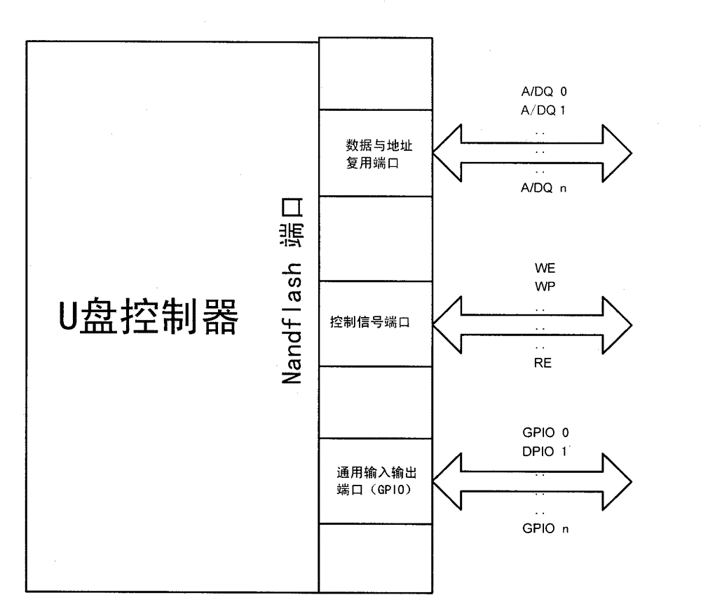
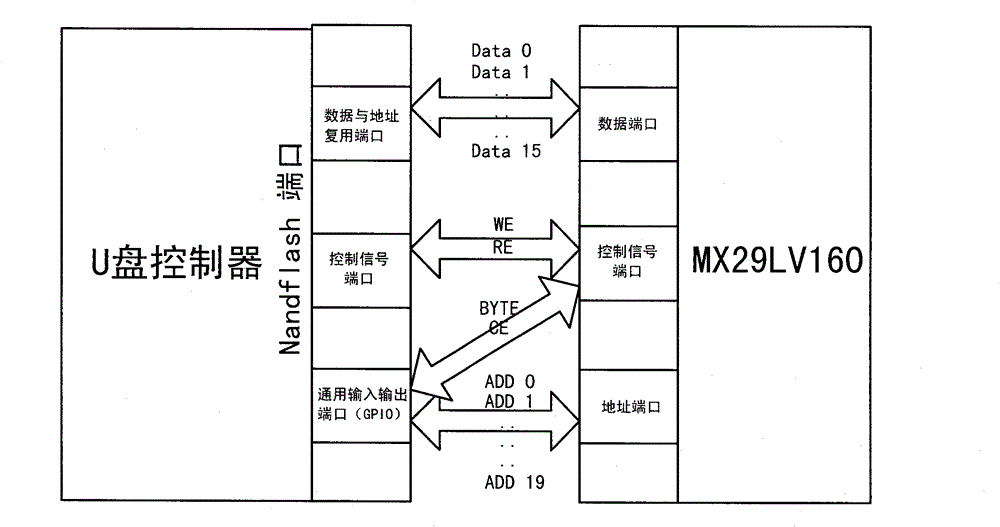
[0021] Such as figure 2 As shown, the port of the existing Nandflash U disk controller is composed of three parts: a data and address multiplexing port, a control signal port and a general-purpose input and output port (GPIO). Among them, the data / address multiplexing port currently only has two types of 8-bit and 16-bit, which are used to provide data input and output and address access; the control signal port provides control signals for operating the Nandflash memory, including the write enable signal (WE) , read enable signal (RE), write protect signal (WP), etc.; general input and output ports (GPIO) provide a set of general GPIO support for different Nandflash types or different customer needs.

[0022] Norflash memory selects MX29LV160 of MXIC. MX29LV160 is a Norflash memory designed with se...

Embodiment 2

[0028] Embodiment 2: a kind of Nandflash U disk controller reads and writes the method for Norflash memory (Norflash memory designed for multiplexing of address line and data line)

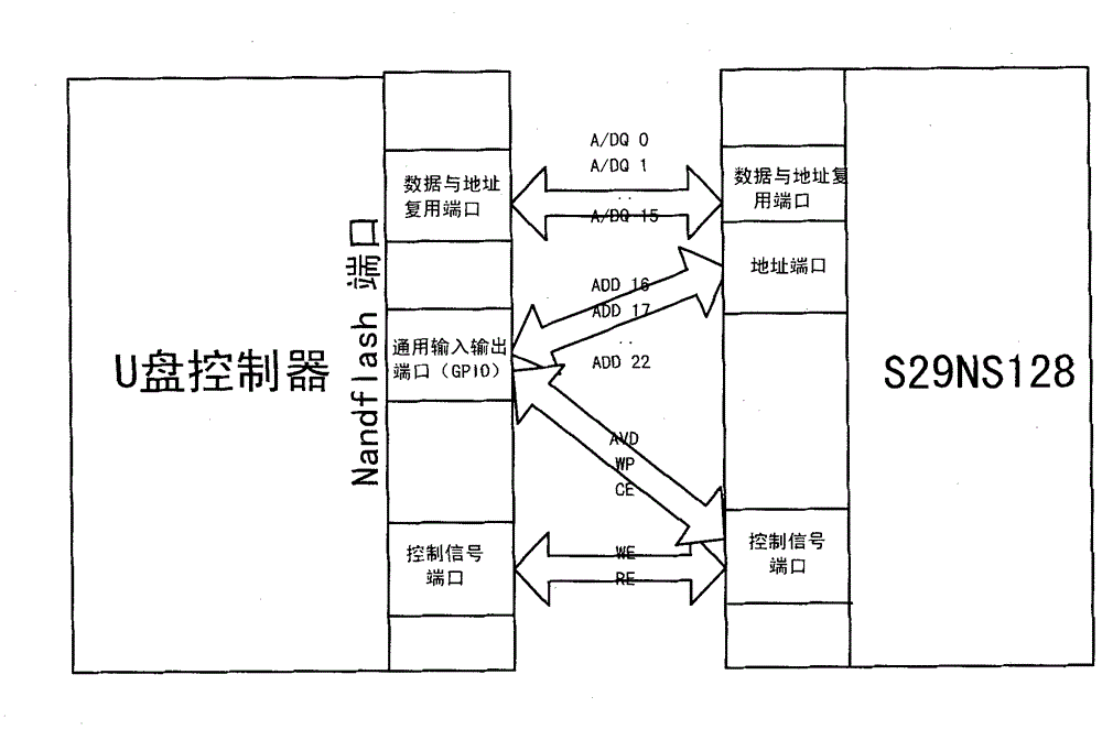
[0029] Such as image 3 As shown, the port of the existing Nandflash U disk controller is composed of three parts: a data and address multiplexing port, a control signal port and a general-purpose input and output port (GPIO). Among them, the data / address multiplexing port currently only has two types of 8-bit and 16-bit, which are used to provide data input and output and address access; the control signal port provides control signals for operating the Nandflash memory, including the write enable signal (WE) , read enable signal (RE), write protect signal (WP), etc.; general input and output ports (GPIO) provide a set of general GPIO support for different Nandflash types or different customer needs.

[0030] Norflash memory selects S29NS128 of Spansion. S29NS128 is a Norflash memory with addre...


PUM


Abstract

The invention relates to a method for a Nandflash USB controller to read and write a Norflash memory, which is characterized in that: using the hardware design of a traditional Nandflash USB controller, for the two situations of the multiplex design and the separated design of an address line and a data line in the Norflash memory, realizing the reading and the writing operation of the Nandflash USB controller to the Norflash memory by re-defining an original connecting port of the Nandflash USB controller and the memory and by adding a software driving program meeting the reading and writing operation time sequence requirements of the Norflash memory. The invention has the beneficial effects that the hardware of the USB controller does not need to be re-designed, the hardware resources of the traditional Nandflash USB controller can be utilized, the reading and the writing to the Norflash memory are realized through software design, thereby not only saving the hardware development cost and time, but also meeting the market demand and achieving very good economy.

Description

technical field [0001] The invention relates to the technical field of U disks, in particular to a method for reading and writing Norflash memory by a Nandflash U disk controller. Background technique [0002] As we all know, U disk is characterized by its small and exquisite portability, large storage capacity, cheap price and reliable performance as a mobile storage device, and is currently widely used by people. Ordinary U disk usually consists of three parts: USB interface, U disk controller and Flash memory. In the common U-disk in the market at present, the memory adopts Nandflash type memory (ie Nandflash memory), and the U-disk controller designed corresponding to the characteristics of the memory is called Nandflash U-disk controller. Such as figure 1 As shown, the port used by the Nandflash U disk controller to connect to the Nandflash memory is usually composed of three parts: a data and address multiplexing port, a control signal port and a general-purpose inpu...

Claims


Application Information

Patent Timeline
Patent Type & Authority Patents(China)
IPC IPC(8): G11C16/26
Inventor 郑茳肖佐楠匡启和王廷平薛毅
Owner 苏州国芯科技股份有限公司
Why Eureka
Try Eureka