Supercharge Your Innovation With Domain-Expert AI Agents!

Thin film deposition apparatus

A thin-film deposition device and thin-film technology, applied in ion implantation plating, metal material coating process, coating, etc., can solve the problems of fine organic thin film formation, difficult manufacturing of driving voltage, current density, color purity, and large luminous efficiency Organic light-emitting display devices, problems such as difficulty

Active Publication Date: 2010-11-24
SAMSUNG DISPLAY CO LTD
View PDF8 Cites 28 Cited by
  • Summary
  • Abstract
  • Description
  • Claims
  • Application Information

AI Technical Summary

Problems solved by technology

However, this structure is difficult to achieve high luminous efficiency, therefore, an intermediate layer including an electron injection layer, an electron transport layer, a hole transport layer, a hole injection layer, etc. is optionally additionally provided between the emission layer and each electrode.
[0005] In addition, it is actually difficult to form fine patterns in organic thin films such as emission layers and interlayers, and red luminous efficiency, green luminous efficiency, and blue luminous efficiency vary depending on the organic thin film
For this reason, it is not easy to form an organic thin film pattern on a large substrate such as a 5G or larger-sized mother glass by utilizing a conventional thin film deposition device, so it is difficult to manufacture driving voltage, current density, brightness, color purity, luminous efficiency, Large-scale organic light-emitting display device with satisfactory lifetime characteristics

Method used


Image

  • Thin film deposition apparatus
  • Thin film deposition apparatus
  • Thin film deposition apparatus

Examples


Embodiment Construction

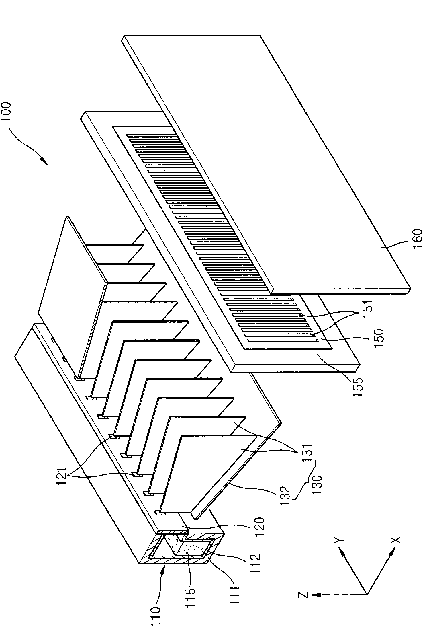
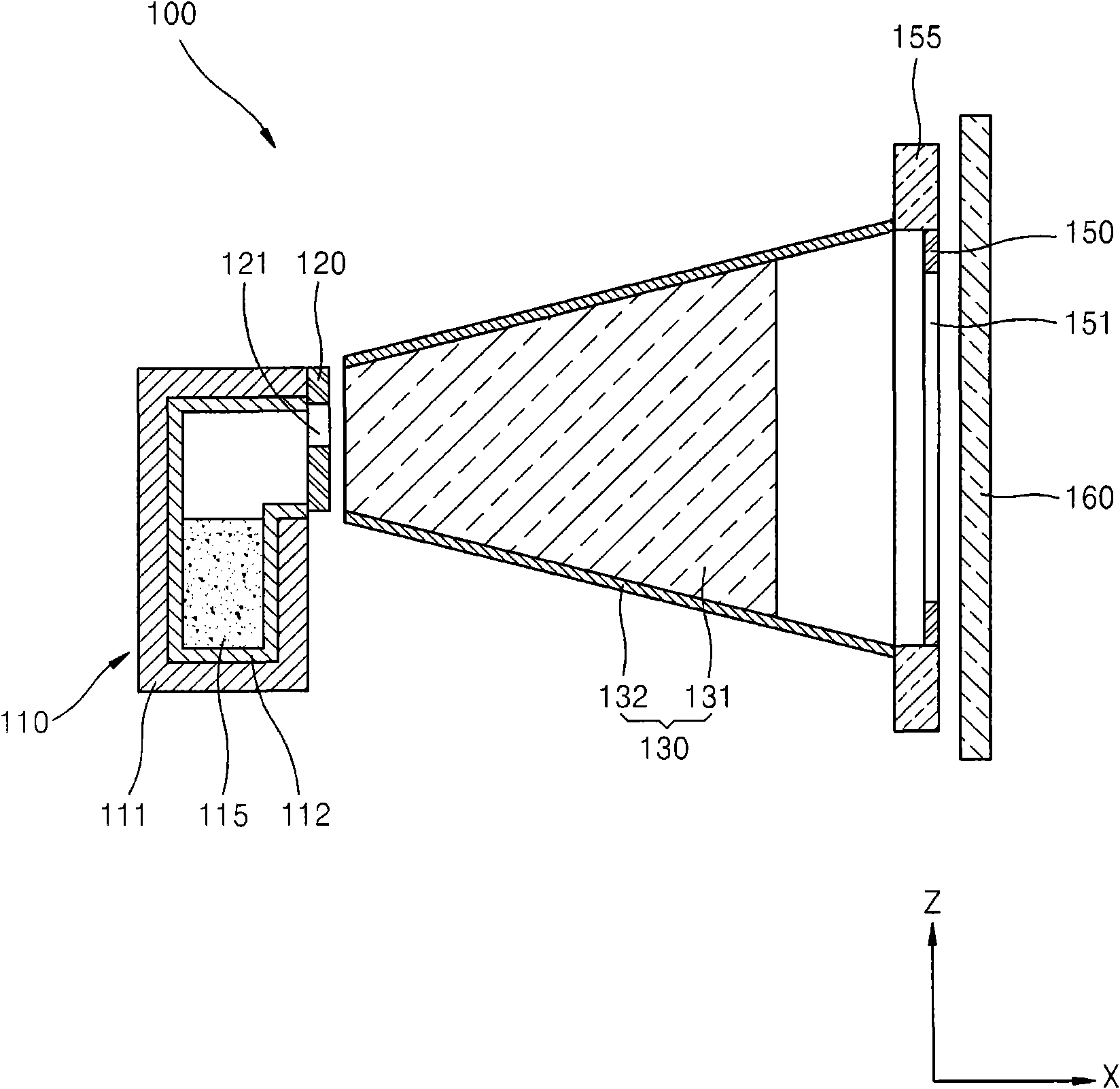
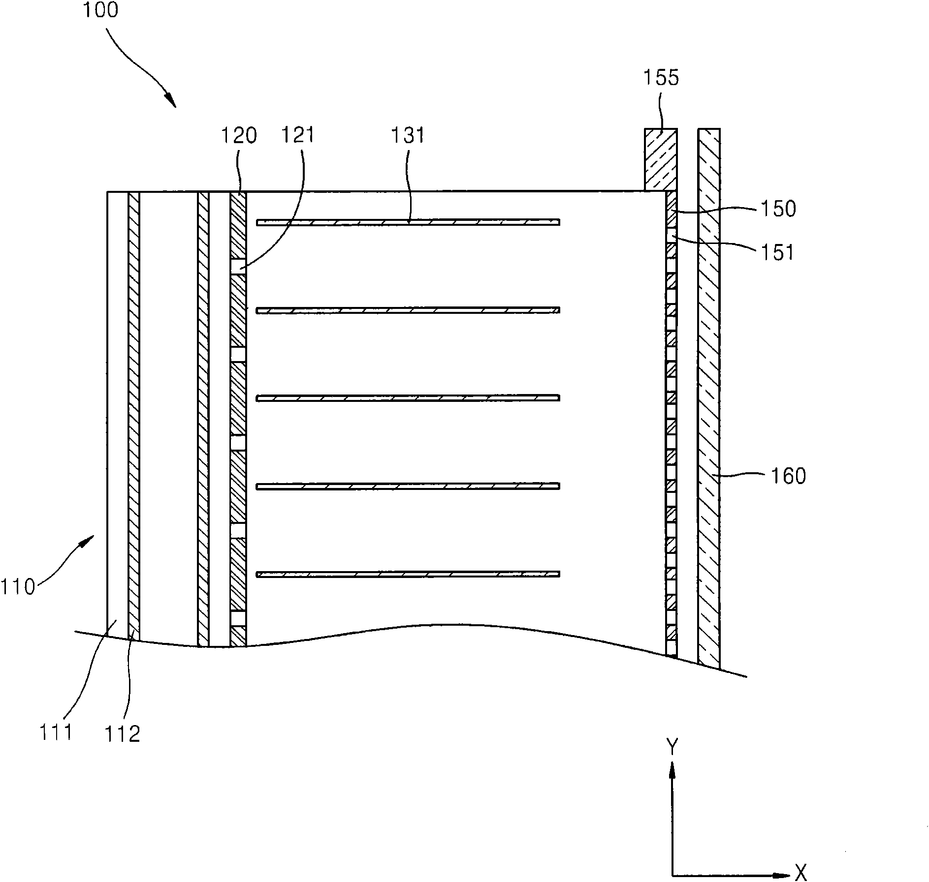
[0089] figure 1 is a schematic perspective view of a thin film deposition apparatus 100 according to an embodiment of the present invention, figure 2 is a schematic side view of the thin film deposition apparatus 100, image 3 is a schematic plan view of the thin film deposition apparatus 100 .

[0090] refer to figure 1 , figure 2 and image 3 , the thin film deposition apparatus 100 according to the current embodiment of the present invention includes a deposition source 110 , a first nozzle 120 , a barrier wall assembly 130 , a second nozzle 150 , a second nozzle frame 155 and a substrate 160 . The thin film deposition apparatus 100 according to the current embodiment of the present invention further includes an interval control member (see Figure 7 ) and alignment control member (see Figure 7 ). will refer to later Figure 7 to Figure 9B The interval control member and the alignment control member will be described in detail.

[0091] Although for ease of expl...


PUM


Abstract

A thin film deposition apparatus that can be simply applied to manufacture large-sized display devices on a mass scale and that improves manufacturing yield includes: a deposition source; a first nozzle disposed at a side of the deposition source and including a plurality of first slits arranged in a first direction; a second nozzle disposed opposite to the first nozzle and including a plurality of second slits arranged in the first direction; a barrier wall assembly including a plurality of barrier walls that are arranged in the first direction in order to partition a space between the first nozzle and the second nozzle; and an alignment member including an interval control member that adjusts an interval between the second nozzle and the substrate, and / or an alignment control member that adjusts alignment between the second nozzle and the substrate.

Description

[0001] This application claims No. 10-2009-0045199 filed with the Korean Intellectual Property Office on May 22, 2009, No. 10-2009-0074001 filed with the Korean Intellectual Property Office on August 11, 2009, and Benefit of Korean Patent Application No. 10-2010-0014272 filed with the Korean Intellectual Property Office on February 17, the disclosures of which are hereby incorporated by reference in their entirety. technical field [0002] The present invention relates to a thin film deposition device, and more particularly, the present invention relates to a thin film deposition device that can be easily used in mass production of large-size display devices and has improved manufacturing yield. Background technique [0003] Compared with other display devices, organic light-emitting display devices have a large viewing angle, good contrast characteristics, and fast response speed, so organic light-emitting display devices are attracting attention as next-generation display d...

Claims


Application Information

Patent Timeline
Patent Type & Authority Applications(China)
IPC IPC(8): C23C14/24C23C14/54
CPCC23C14/24
Inventor 李忠浩李廷敏
Owner SAMSUNG DISPLAY CO LTD
Features
  • R&D
  • Intellectual Property
  • Life Sciences
  • Materials
  • Tech Scout
  • Unparalleled Data Quality
  • Higher Quality Content
  • 60% Fewer Hallucinations
Learn More