LED encapsulation method and LED encapsulation structure encapsulated with same

A technology of LED packaging and LED chips, which is applied in the direction of electrical components, electric solid devices, circuits, etc., can solve the problems of low light output efficiency of LED package structure, and achieve the effects of benefiting light output, improving light output efficiency, and reducing light absorption

Inactive Publication Date: 2010-12-15
SHENZHEN REFOND OPTOELECTRONICS
View PDF5 Cites 22 Cited by
  • Summary
  • Abstract
  • Description
  • Claims
  • Application Information

AI Technical Summary

Problems solved by technology

[0003] The purpose of the embodiments of the present invention is to provide an LED packaging method, aiming to solve th

Method used


Image

  • LED encapsulation method and LED encapsulation structure encapsulated with same
  • LED encapsulation method and LED encapsulation structure encapsulated with same
  • LED encapsulation method and LED encapsulation structure encapsulated with same

Examples


Example Embodiment

[0033] Embodiment one:

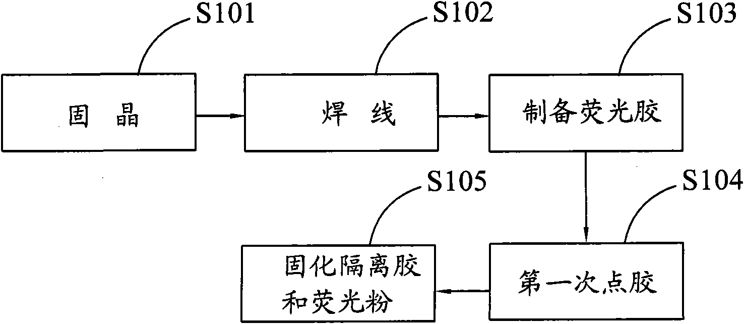
[0034] figure 1 and Figure 3 ( Figures 3a-3d ) shows a flow chart and a schematic diagram of the operation of the LED packaging method provided by the first embodiment of the present invention, and is described in detail as follows:

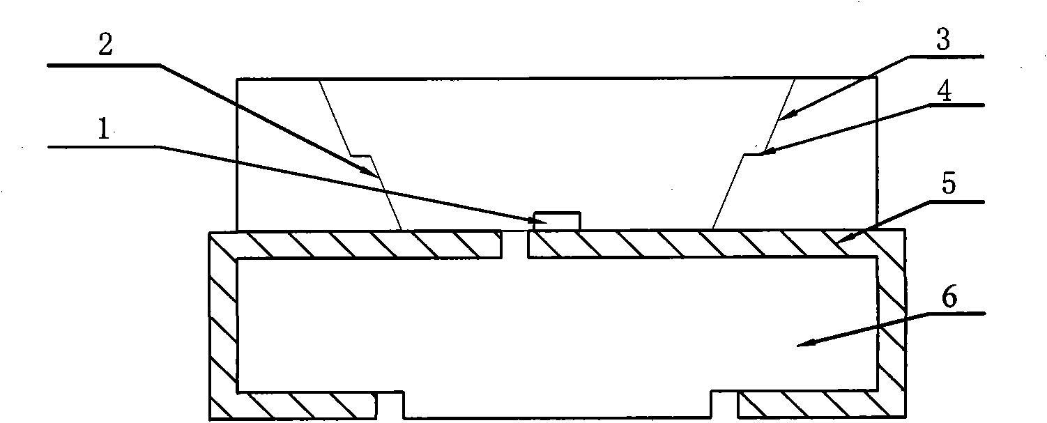
[0035] In step S101, the LED chip 1 is fixed on the lead frame 5 of the LED bracket, such as Figure 3a ;

[0036] In step S102, the two ends of the bonding wire 7 are respectively connected to the LED chip 1 and the lead frame 5, so that the LED chip 1 and the lead frame 5 are electrically connected, as Figure 3b ;

[0037] In step S103, evenly mix the isolation glue 9 and the fluorescent powder to prepare the fluorescent glue 8;

[0038] In step S104, the first glue dispensing is performed, and the fluorescent glue 8 is put into the reflective cup to cover the LED chip 1, such as Figure 3c ;

[0039] In step S105, the fluorescent powder and the isolation glue 9 are cured, and the LED bracket after the first ...

Example Embodiment

[0041] Embodiment two:

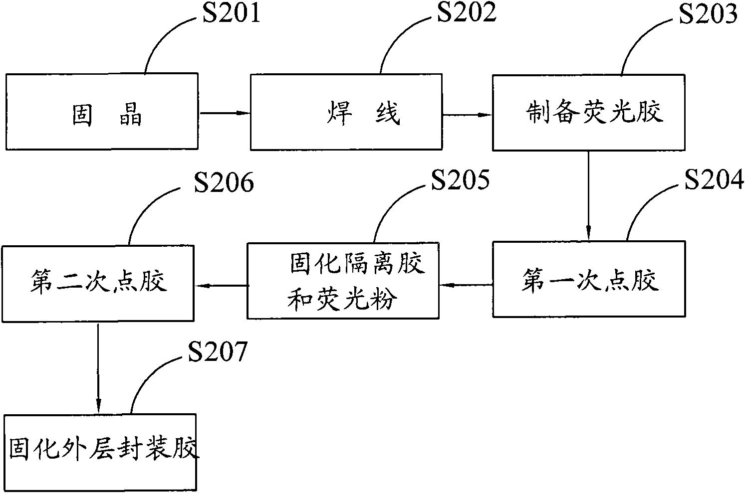
[0042] figure 2 and Figure 3 ( Figures 3a-3e ) shows a flow chart and a schematic diagram of the operation of the LED packaging method provided in the second embodiment of the present invention, which are described in detail as follows:

[0043] The embodiment of the present invention is a further optimization of the LED packaging method provided in the first embodiment above. Steps S201 to S205 are the same as steps S101 to S105 in the first embodiment above. After step S205, the following steps are added:

[0044] In step S206, after the baked LED bracket is turned over, the second dispensing is performed, such as Figure 3e .

[0045] Cover the outer layer encapsulation glue 11 on the outside of the crescent-shaped phosphor layer 10 to protect the phosphor layer 10. By selecting the insulating glue 9 and the outer layer encapsulating glue 11 with suitable bonding performance, the insulating glue 9 and the outer layer encapsulation can be made...

Example Embodiment

[0047] Embodiment three:

[0048] The embodiment of the present invention specifically sets the baking conditions in the above-mentioned embodiment 1 or embodiment 2. The time for baking the LED bracket after the first dispensing is 6 hours, and the baking temperature is 25°C.


PUM

PropertyMeasurementUnit
Densityaaaaaaaaaa
Particle sizeaaaaaaaaaa
Viscosityaaaaaaaaaa

Abstract

The invention is suitable for LED encapsulation field and provides an LED encapsulation method and an LED encapsulation structure encapsulated with the same. The method comprises the following steps of: die bonding: fixing an LED chip on a lead frame of an LED bracket; wire bonding: electrically connecting the LED chip and the lead frame via a bonding wire; preparation of fluorescent glue: evenly mixing insulation glue and phosphor powder to prepare the fluorescent glue; glue dispensation for the first time: dispensing the fluorescent glue into a reflection cup so as to cover the LED chip; and solidification of the phosphor powder and the insulation glue: inverting the LED bracket subjected to the first glue dispensation and baking so as to form a crescent phosphor powder layer far away from the LED chip. The invention employs an anti-deposition encapsulation technology to perform LED encapsulation, thereby solving the problem that the over-high temperature caused by long-term contact between the phosphor powder and the chip influences the luminous efficiency, reducing the light loss caused by scattering and interface light loss, and improving the extraction efficiency of the LED.

Description

technical field [0001] The invention belongs to the field of LED packaging, in particular to an LED packaging method and an LED packaging structure packaged by the method. Background technique [0002] With the continuous development of LED in the lighting field, people have higher and higher requirements for its light extraction efficiency, and the packaging structure of LED is the main factor affecting the light extraction efficiency. At present, most white LEDs are packaged by covering the blue light chip with encapsulant, and the phosphor powder is evenly distributed in the encapsulant. When this encapsulation method is adopted, the light emitted by the phosphor is scattered many times, making its emission route longer. The absorption of light is increased, resulting in a decrease in light extraction efficiency. There are also some packaging structures where the phosphor powder is closely attached to the surface of the chip, and the heat of the chip is directly transmit...

Claims


Application Information

Patent Timeline
IPC IPC(8): H01L33/48H01L33/50H01L33/56H01L33/60
CPCH01L2224/48091H01L2224/48247H01L2924/181H01L2924/00014H01L2924/00012
Inventor 肖兆新
Owner SHENZHEN REFOND OPTOELECTRONICS
Why Eureka
Try Eureka