Thin wafer handling structure, and thin wafer bounding and releasing method

A technology of thin wafers and wafers, which is applied in the field of thin wafer processing structure and easy bonding and stripping, which can solve the problems of high stripping temperature and the influence of internal wiring configuration, etc., and achieve the effect of good chemical resistance

Active Publication Date: 2013-04-03
TAIWAN SEMICON MFG CO LTD
View PDF0 Cites 0 Cited by
  • Summary
  • Abstract
  • Description
  • Claims
  • Application Information

AI Technical Summary

Problems solved by technology

This method requires a higher stripping temperature and adversely affects the interconnection scheme

Method used


Image

  • Thin wafer handling structure, and thin wafer bounding and releasing method
  • Thin wafer handling structure, and thin wafer bounding and releasing method

Examples


Embodiment Construction

[0016] The methods of making and using various embodiments of the present invention will be discussed in detail below. However, it is worth noting that many feasible inventive concepts provided by the present invention can be implemented in various specific ranges. These specific embodiments are only used to illustrate the manufacturing and use methods of the present invention, but are not used to limit the scope of the present invention.

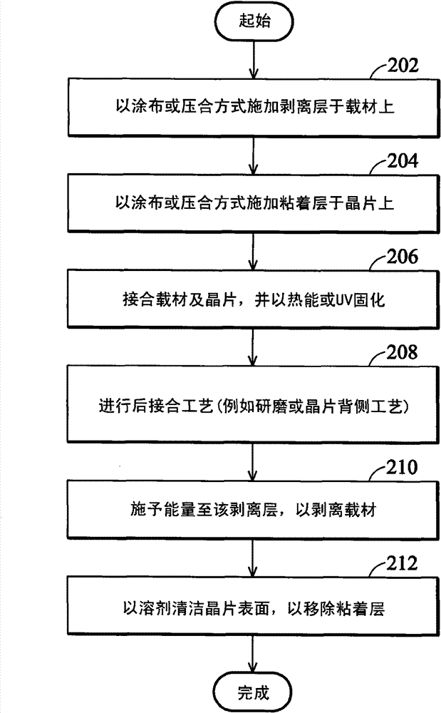
[0017] The invention provides a thin wafer processing structure and method to facilitate bonding and peeling in the wafer process. In the various illustrations and embodiments disclosed in the present invention, similar signs are used to indicate similar elements.

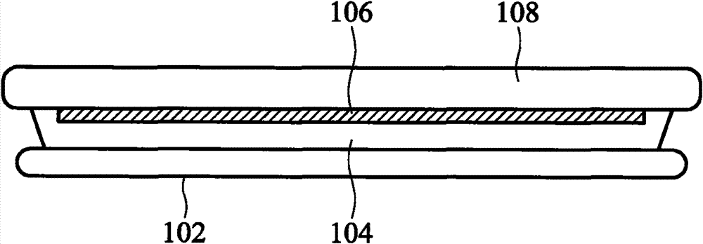
[0018] figure 1 It is shown as a thin wafer processing structure according to an embodiment of the present invention to facilitate bonding and peeling. The wafer 102 is bonded to the carrier 108 by using two film layers (ie, the peeling layer 106 and the adhesive layer 104) between...


PUM


Abstract

A thin wafer handling structure includes a semiconductor wafer, a release layer that can be released by applying energy, an adhesive layer that can be removed by a solvent, and a carrier, where the release layer is applied on the carrier by coating or laminating, the adhesive layer is applied on the semiconductor wafer by coating or laminating, and the semiconductor wafer and the carrier is bonded together with the release layer and the adhesive layer in between. The method includes applying a release layer on a carrier, applying an adhesive layer on a semiconductor wafer, bonding the carrier and the semiconductor wafer, releasing the carrier by applying energy on the release layer, e.g. UV or laser, and cleaning the semiconductor's surface by a solvent to remove any residue of the adhesive layer.

Description

Technical field [0001] The invention relates to wafer processing, in particular to a thin wafer processing structure and a method for facilitating bonding and peeling. Background technique [0002] In the semiconductor wafer processing process, the backside process of the thin wafer requires temporary bonding and stripping techniques. The wafer is bonded to a rigid carrier through an adhesive layer. After grinding and / or other post-bonding processes, the wafer is peeled off from the rigid carrier. [0003] One of the traditional peeling methods is to use a laser on a light-to heat conversion layer to peel off the carrier, and then peel off the adhesive layer. The adhesive material is an ultraviolet (UV) curing material, such as a thermosetting polymer that cannot be stripped by chemicals, but can be peeled off physically. This method will leave chemical residues after the wafer is peeled off. Therefore, the laser lift-off layer has extremely low chemical resistance during the b...

Claims


Application Information

Patent Timeline
Patent Type & Authority Patents(China)
IPC IPC(8): H01L23/00H01L21/20H01L21/78
CPCH01L2221/68318H01L2221/68327H01L21/6835H01L2221/68381H01L21/187Y10T428/1476
Inventor 余振华许国经陈承先萧景文
Owner TAIWAN SEMICON MFG CO LTD
Why Eureka
Try Eureka