

Logic block management method for flash memory as well as control circuit and storage system thereof
A technology for flash memory and memory management, which is applied in the field of flash memory control circuits and flash memory storage systems, and can solve problems such as shortened life of flash memory storage devices
- Summary
- Abstract
- Description
- Claims
- Application Information
AI Technical Summary
Problems solved by technology
Method used
Image

Examples
Embodiment Construction
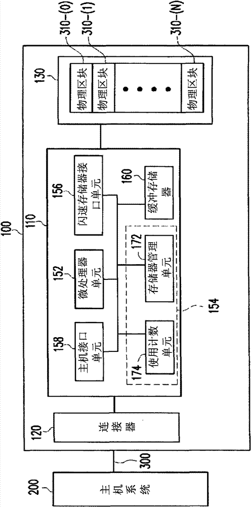
[0037] figure 1 It is a schematic block diagram of a flash memory storage system shown in an embodiment of the present invention.
[0038] Please refer to figure 1 Generally, the flash memory storage device 100 is used together with the host system 200 so that the host system 200 stores data into the flash memory storage device 100 or reads data from the flash memory storage device 100 . In this embodiment, the flash memory storage device 100 is a solid state drive (SSD for short). However, it must be understood that in another embodiment of the present invention, the flash memory storage device 100 may also be a memory card or a pen drive.
[0039]The flash memory storage device 100 includes a flash memory controller (also called a flash memory control circuit) 110 , a connector 120 and a flash memory chip 130 .
[0040] The flash memory controller 110 executes a plurality of logic gates or control instructions implemented in hardware or software, and writes, reads, and er...
PUM
 Abstract
Description
Claims
Application Information