Nonvolatile storage system, power supply circuit for memory system, flash memory, flash memory controller, and nonvolatile semiconductor storage device

a technology of power supply circuit and memory system, which is applied in the direction of memory address/allocation/relocation, instruments, liquid/fluent solid measurement, etc., can solve the problems of degrading data reliability in flash memory, hardly succeeding in executing processes in target cells, etc., and achieves less power usage, stable execution of process, and less power usage

Active Publication Date: 2013-05-16
PANASONIC SEMICON SOLUTIONS CO LTD
View PDF11 Cites 111 Cited by
  • Summary
  • Abstract
  • Description
  • Claims
  • Application Information

AI Technical Summary

Benefits of technology

[0048]<50> Functionally describing the main structural elements of the nonvolatile storage system according to the invention, provided are: a memory block having a plurality of flash memories provided as a nonvolatile storage device; a flash memory controller for controlling execution of a process in each of the plurality of flash memories; and a power supply circuit for supplying the plurality of flash memories with power to enable operations of the flash memories. It is the minimum requirement to provide three structural elements (memory block, flash memory controller, and power supply circuit). According to the invention, the nonvolatile storage system per se is equipped with the power supply circuit for memory system. Thus, the nonvolatile storage system is different to any conventional system designed to receive power from a host-side power supply circuit. The power supply circuit for memory system provided outside of the memory block, which is different to any conventional system where each flash memory has therein a power supply circuit.
[0049]Some flash memories are configured for data reading, writing, and erasing, while some flash memories are further configured for verifying whether data is written or erased. The invention imposes no restrictions on the spec of the flash memory.
[0050]The internal circuit configuration of the power supply circuit for memory system conforms to the spec of the flash memory. The power supply circuit for memory system may include a power supply circuit for reading and also a power supply circuit for writing/erasing. The power supply circuit for memory system may further include a power supply circuit for verifying data writing/erasing. The invention imposes no restrictions on the internal circuit configuration.
[0051]In the nonvolatile storage system wherein the power supply circuit for memory system is shared by the plural flash memories and t...

Problems solved by technology

However, it hardly succeeds to complete the processes respectively executed in the target cells in a single attempt by simply injecting and withdrawing electric charges to and from flo...

Method used


Image

  • Nonvolatile storage system, power supply circuit for memory system, flash memory, flash memory controller, and nonvolatile semiconductor storage device
  • Nonvolatile storage system, power supply circuit for memory system, flash memory, flash memory controller, and nonvolatile semiconductor storage device
  • Nonvolatile storage system, power supply circuit for memory system, flash memory, flash memory controller, and nonvolatile semiconductor storage device

Examples


working example 1

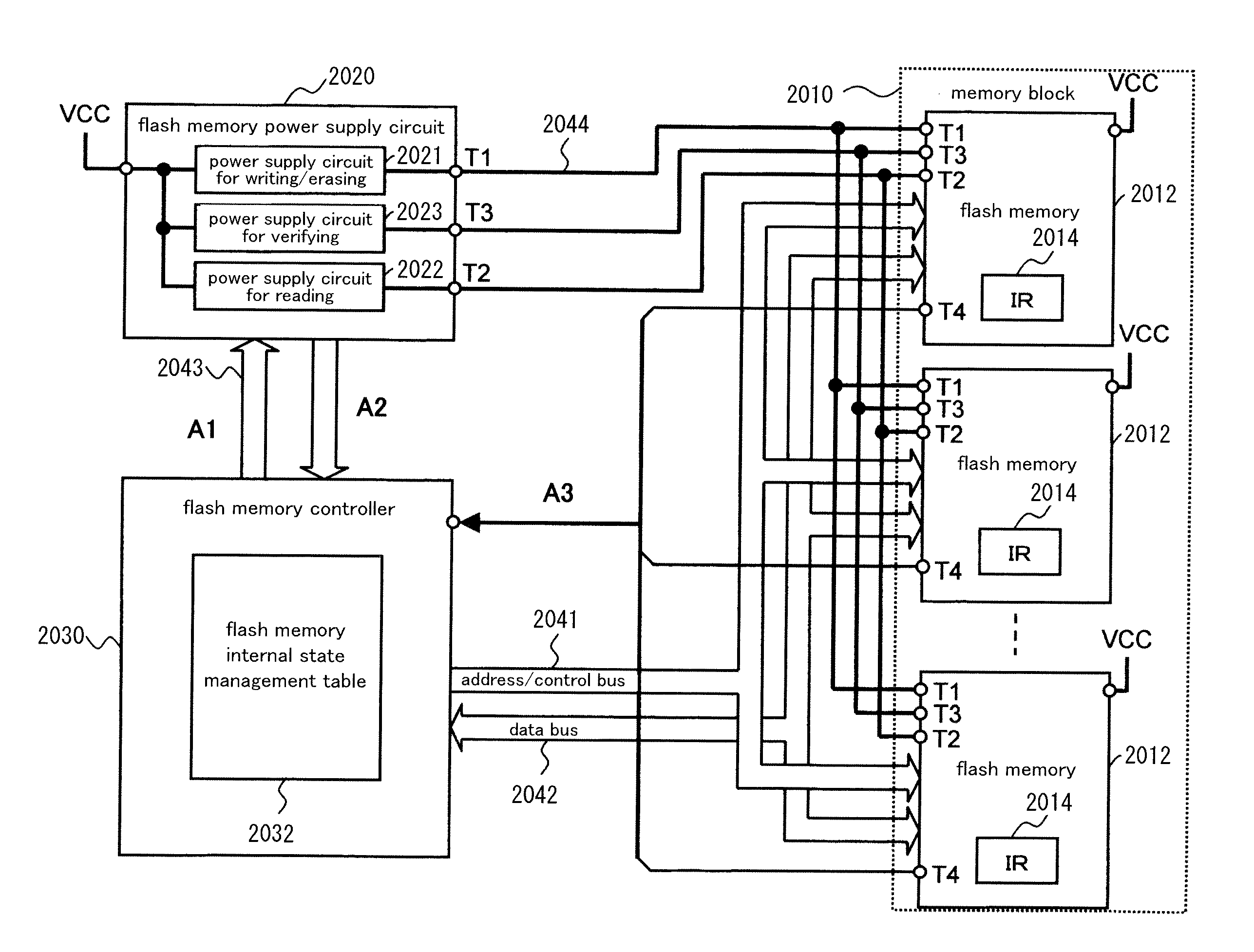
[0224]FIG. 1 is a block diagram illustrating structural characteristics of a nonvolatile storage system according to a working example 1 of the invention. The nonvolatile storage system according to the working example includes a memory block 2010 having a plurality of flash memories 2012, a flash memory power supply circuit 2020, and a flash memory controller 2030. The flash memory power supply circuit 2020 and the flash memory controller 2030 may be different semiconductor devices independent from each other or may be semiconductor devices integrally mounted on a chip.

[0225]The flash memory controller 2030 is connected to the flash memories 2012 by an address / control bus 2041 and a data bus 2042. The flash memory controller 2030 is connected to the flash memory power supply circuit 2020 by a control bus 2043. The flash memory power supply circuit 2020 is connected to the flash memories 2012 by power supply lines 2044.

[0226]None of the flash memories 2012 is embedded with a power s...

working example 2

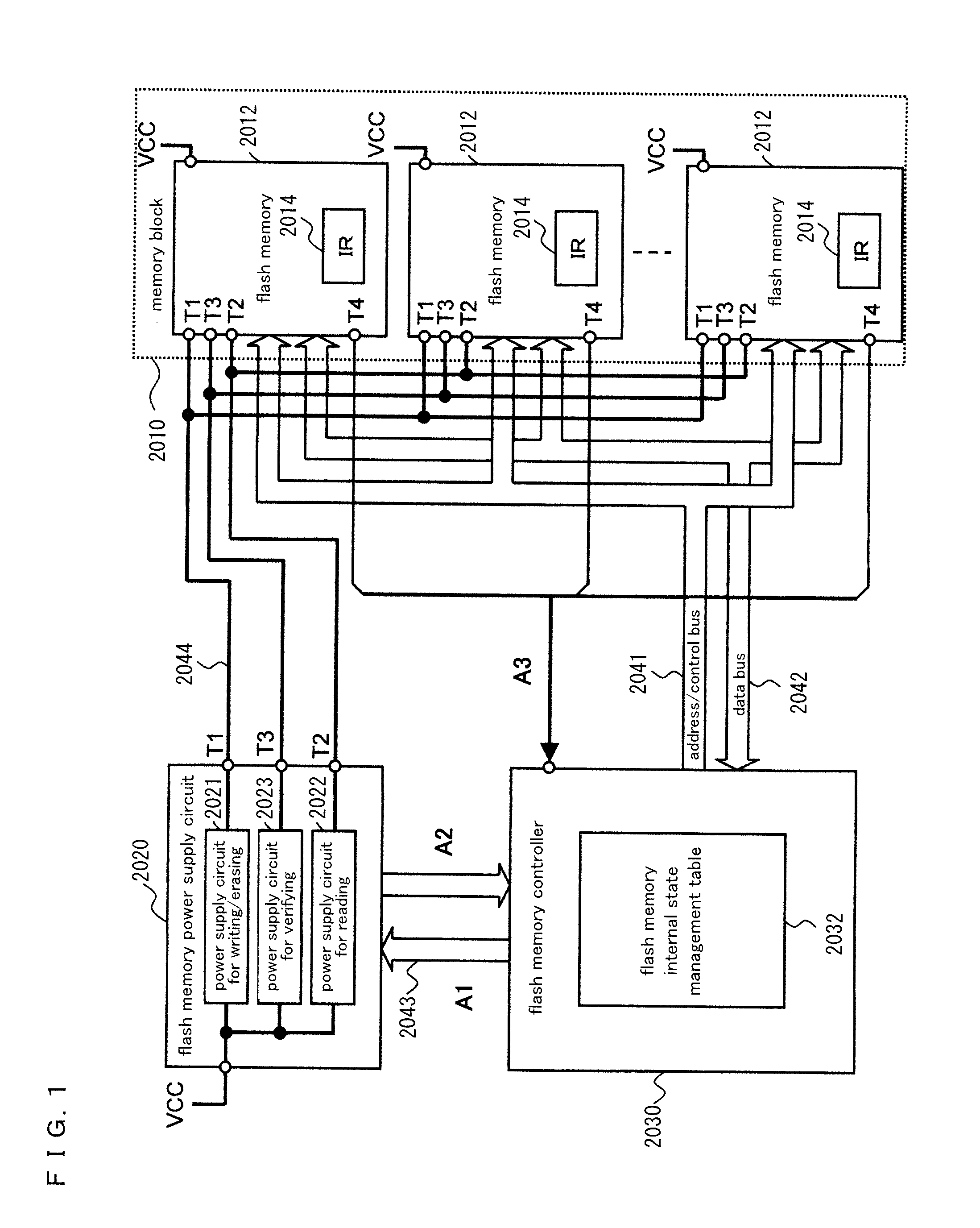
[0303]FIG. 7 is a block diagram illustrating structural characteristics of a nonvolatile storage system according to a working example 2 of the invention. The information indicated by an information register 2014 of the flash memory 2012 includes, in addition to the operating state (process being executed) currently executed by the internal controller (not illustrated in the drawing) of the flash memory 2012, information of power supply voltages for reading, writing / erasing, and verifying. This information indicates the power supply voltages necessary for the flash memory 2012 to operate. The flash memories 2012 each has an optimal power supply voltage information. There are individual differences among the flash memories, which are generated by, for example, manufacturing tolerances.

[0304]To notify the applied voltage information, an applied voltage notifying signal A32, for example, is used. This signal may be directly connected to the flash memory controller 2030. T6 is an output...

working example 3

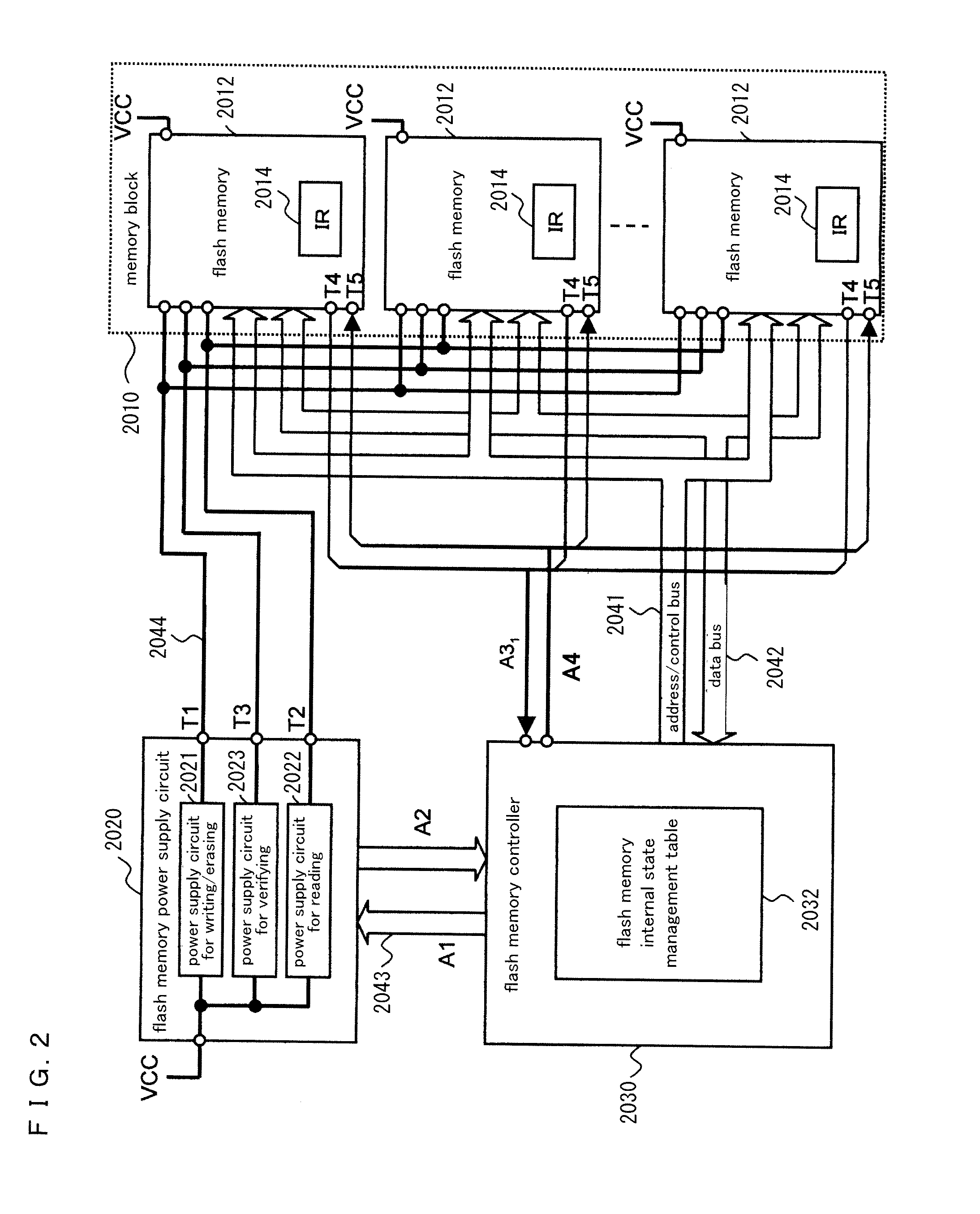
[0319]FIG. 9 is a block diagram illustrating structural characteristics of a nonvolatile storage system according to a working example 3 of the invention. The flash memory internal state management table 2032 of the flash memory controller 2030 is provided with an applied voltage information storage 2033, in which the applied voltage informations of the flash memories 2012 are stored. The applied voltage informations may be collected in the flash memory internal state management table 2032 by issuing the internal state reading command for all of the flash memories 2012 at the time of startup of the system, or the voltage applied information of each flash memory 2012 may be collected every time when the flash memory 2012 is accessed and stored in the flash memory internal state management table 2032.

[0320]According to the working example, all of the applied voltage informations are read at once at the time of startup of the system. With reference to a flow chart illustrated in FIG. 1...


PUM


Abstract

Disclosed is a nonvolatile storage system including: a memory block having a plurality of flash memories; a flash memory power supply circuit outside of the memory block; and a flash memory controller. The flash memory power supply circuit has a plurality of types of power supply circuits for process execution, the power supply circuits for process execution generating and supplying power at a plurality of voltage levels needed to execute processes in the flash memories. The flash memory controller monitors changes of the internal states of the flash memories by communicating with the flash memories, thereby controlling the power supply circuits for process execution and the flash memories.

Description

TECHNICAL FIELD[0001]The invention relates to a nonvolatile storage system provided with a nonvolatile storage device such as a SSD (Solid State Drive) or SD (Secure Digital) memory card in which a plurality of flash memories are used. The invention more particularly relates to a technology for reducing power consumption in a more advantageous manner in such an operating environment that running states of processes in a plurality of flash memories are dynamically changing, the invention further relating to a technology for ensuring a high data reliability through an operational stability by avoiding system crash caused by unfavorable events, such as overload, in a power supply circuit for memory system where a state of power supply is undergoing dynamic changes.BACKGROUND ART[0002]In recent years, storage devices configured for fast data processes, for example, SD memory card and memory stick, are becoming increasingly popular among consumers. These nonvolatile storage devices, in w...

Claims


Application Information

Patent Timeline
IPC IPC(8): G06F1/32G06F12/02
CPCG11C16/30G11C16/06G06F12/0246G11C16/34G06F1/3225
Inventor TANAKA, TAKAYUKISAKAI, KEISUKEMATSUMOTO, MAKOTOMORI, TOSHIKITOMITA, YASUHIROYAMAHIRA, SEIJI
Owner PANASONIC SEMICON SOLUTIONS CO LTD
Why Eureka
Try Eureka