Oled display panel with PWM control

A technology for display panels and driving transistors, applied to static indicators, instruments, etc., can solve problems such as difficulty in reducing costs and complicated transistor manufacturing process

Active Publication Date: 2011-02-16
GLOBAL OLED TECH
View PDF1 Cites 12 Cited by
  • Summary
  • Abstract
  • Description
  • Claims
  • Application Information

AI Technical Summary

Problems solved by technology

However, these measures complicate the manufacturing process of transistors, which makes it difficult to reduce costs

Method used


Image

  • Oled display panel with PWM control
  • Oled display panel with PWM control
  • Oled display panel with PWM control

Examples


Embodiment Construction

[0017] Hereinafter, embodiments of the present invention will be described with reference to the accompanying drawings.

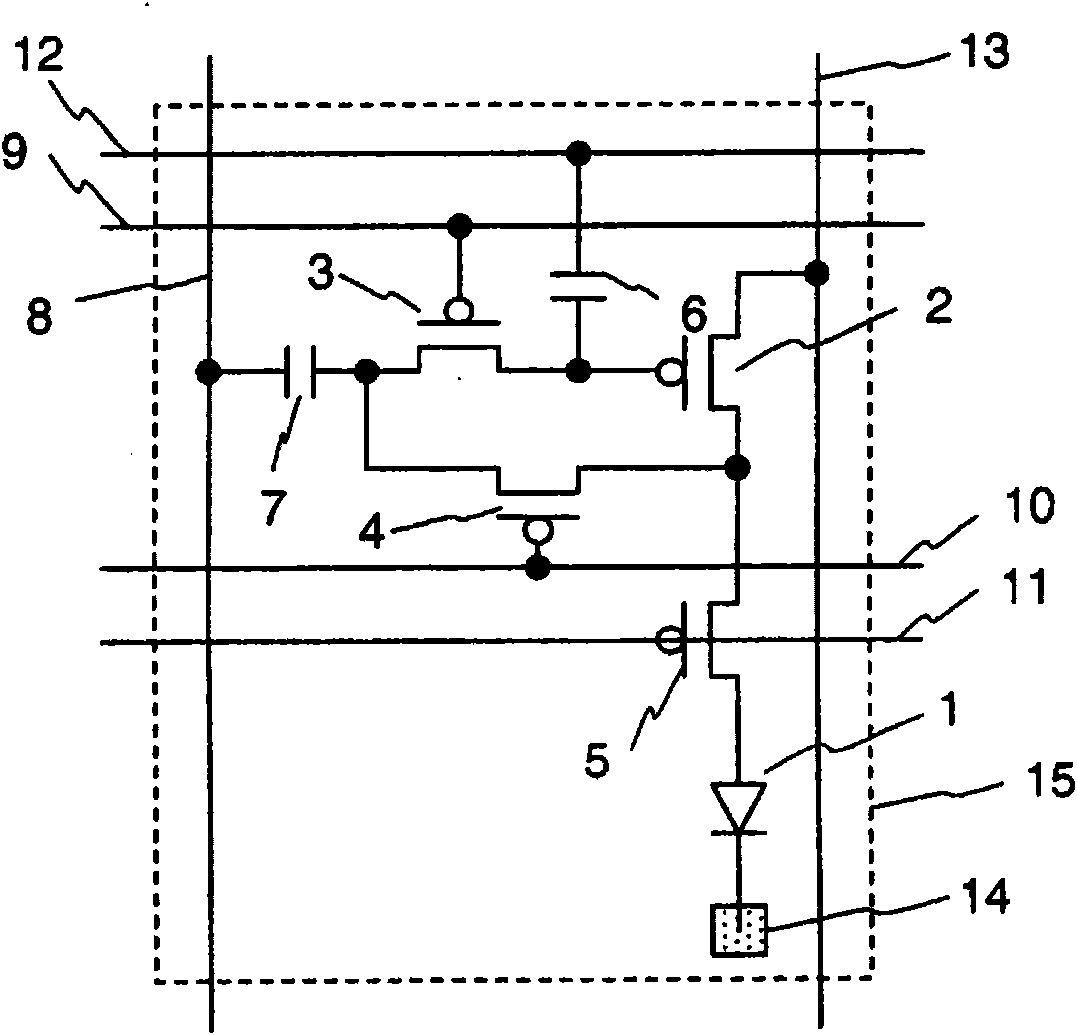
[0018] figure 1 An exemplary structure of a pixel 15 in a display according to an embodiment is shown in . The pixel 15 includes an organic EL element 1 , a drive transistor 2 , a selection transistor 3 , a reset transistor 4 , an emission control transistor 5 , a storage capacitor 6 , and a coupling capacitor 7 . It should be noted that each transistor uses a P-type thin film transistor.

[0019] The drive transistor 2 is constructed such that its source terminal is connected to the power supply line 13 shared by all pixels, its drain terminal is connected to the source terminal of the light emission control transistor 5 and the source terminal of the reset transistor 4, and its gate terminal is connected to the storage capacitor 6 One terminal of the storage capacitor 6 is connected to the source terminal of the selection transistor 3 , and the other te...


PUM


Abstract

A display panel which applies a PWM drive to a drive transistor (2) is provided. A drive transistor supplies current in accordance with its gate voltage, and the current is supplied to a light-emitting element (1) to illuminate the light emitting element. One end of a storage capacitor (6) is connected to the gate of the drive transistor, while the other end thereof is connected to a sweep line (12). A triangular wave which alternately repeats an up phase and a down phase is supplied to the sweep line in order to control an on period of the drive transistor in accordance with the gate voltage, thereby controling light emission of the light-emitting element.

Description

technical field [0001] The invention relates to a display panel having pixels arranged in a matrix. Background technique [0002] Because organic EL displays are self-luminous, they exhibit high contrast and fast response, making them suitable for video applications such as televisions displaying natural images and the like. In general, organic EL elements are driven by controlling elements such as transistors by driving the transistors with a constant current according to data, or by driving the transistors with a constant voltage to achieve multi-tone to change the light emission period. [0003] In the case of driving transistors with a constant current, since they are used in a saturation region, changes in transistor characteristics such as threshold and mobility cause changes in current flowing through the organic EL element, which causes non-uniformity in display. Therefore, JP2007-79599A discloses a method of reducing non-uniformity in display by digitally driving t...

Claims


Application Information

Patent Timeline
Patent Type & Authority Applications(China)
IPC IPC(8): G09G3/20G09G3/32
CPCG09G3/3258G09G2300/0852G09G2300/0861G09G3/2014G09G2320/043G09G3/3266G09G3/3233G09G2310/066G09G2300/0819G09G2300/0876
Inventor 川边和佳
Owner GLOBAL OLED TECH
Why Eureka
Try Eureka