Wiring substrate

A wiring board and wiring technology, which is applied to printed circuits, printed circuit parts, electrical components, etc., can solve the problems of changing the shape and area of ​​wiring, difficulties, etc., and achieve the effect of good transmission characteristics

Inactive Publication Date: 2011-03-23
KK TOSHIBA
View PDF1 Cites 1 Cited by
  • Summary
  • Abstract
  • Description
  • Claims
  • Application Information

AI Technical Summary

Problems solved by technology

Therefore, it is difficult to change the shape and area of ​​wiring
Furthermore, the signal to be supplied to the circuit is very high-speed, and further improvement in transmission characteristics is required

Method used


Image

  • Wiring substrate
  • Wiring substrate
  • Wiring substrate

Examples


Embodiment Construction

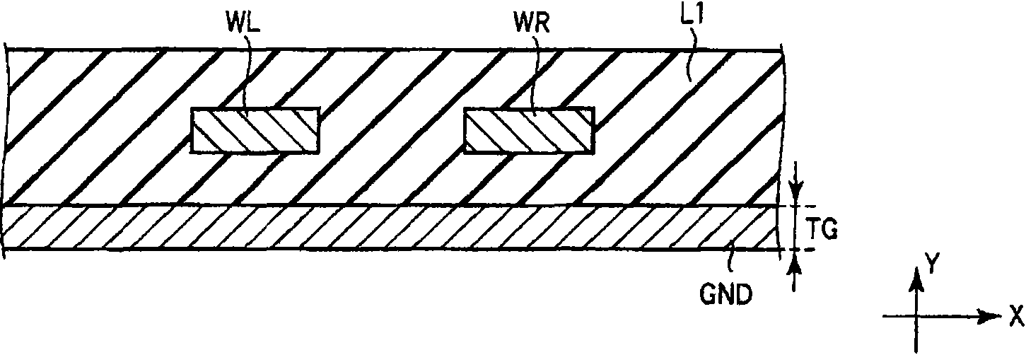
[0018] Hereinafter, a wiring board according to a first embodiment of the present invention will be described. Such as figure 1 As shown, the wiring board of the present embodiment has a ground layer GND supplied with a ground potential, and first wiring WL and second wiring WR arranged on the ground layer GND through an insulating layer L1. The ground layer GND is disposed in a planar manner on the substrate surface of the wiring substrate of the present embodiment. exist figure 1 In the shown cross section, the first wiring WL and the second wiring WR are arranged side by side in the X direction.

[0019] In this embodiment, the first wiring WL and the second wiring WR are formed of copper, for example. The ground layer GND is formed of a material having a higher resistivity than the first wiring WL and the second wiring WR. In the present embodiment, the ground layer GND is formed of, for example, a high-resistance material having a resistance higher than that of copper...


PUM

PropertyMeasurementUnit
Thicknessaaaaaaaaaa

Abstract

The present invention provides a wiring substrate with unchanged shape and area and excellent transmission characteristic. The wiring substrate comprises the following components: a ground layer (GND) which is supplied with a ground potential; an insulation layer (L1) which is configured on the ground layer (GND); a first wiring (WL) and a second wiring (WR) which are configured oppositely with the ground layer through the insulation layer (L1) and transmit signal through a differential transmission mode, wherein the ground layer (GND) is made of material which has resistivity that is higher than those of the first wiring (WL) and the second wiring (WR).

Description

technical field [0001] The present invention relates to a wiring board, and more particularly, to a wiring board having a ground layer provided with a ground potential and wiring for transmitting signals by a differential transmission method. Background technique [0002] The transmission speed of data used in portable computers is increasing day by day. The requirement for high-speed transmission characteristics of the wiring board for transmitting signals has also reached a high level. In recent years, wiring boards such as flexible printed wiring boards (FPC) have been used in parts where high-speed signals are used, such as the connection between a main board and a hard disk drive (HDD). [0003] For example, Patent Document 1 proposes a substrate having a shield plane with various opening patterns for controlling transfer time and impedance. In the substrate disclosed in this document, characteristic impedance control or propagation delay control is performed by chang...

Claims


Application Information

Patent Timeline
IPC IPC(8): H05K1/00H05K1/02
Inventor 鸟越保辉
Owner KK TOSHIBA
Why Eureka
Try Eureka