Electromagnetic shielding effect multi-field coupling simulation method for electronic device chassis with conductive rubber

A technology of conductive rubber and electronic equipment, applied in the fields of magnetic/electric field shielding, electrical components, electrical digital data processing, etc., which can solve problems such as large errors and difficult simulations

Inactive Publication Date: 2011-04-06
XIDIAN UNIV
View PDF4 Cites 22 Cited by
  • Summary
  • Abstract
  • Description
  • Claims
  • Application Information

AI Technical Summary

Problems solved by technology

[0008] The purpose of the present invention is to solve the problem of difficulty in simulation and relatively large errors due to numerous influencing factors in the simulation of the electromagnetic screen effect of the electronic equipment chassis at present, and proposes a multi-field coupling simulation method for the electromagnetic screen effect of the electronic equipment chassis with conductive rubber to realize The accurate simulation of the electromagnetic screen effect of the electronic equipment chassis under the influence of multiple factors provides a reference for the design of the chassis structure

Method used


Image

  • Electromagnetic shielding effect multi-field coupling simulation method for electronic device chassis with conductive rubber
  • Electromagnetic shielding effect multi-field coupling simulation method for electronic device chassis with conductive rubber
  • Electromagnetic shielding effect multi-field coupling simulation method for electronic device chassis with conductive rubber

Examples


Embodiment Construction

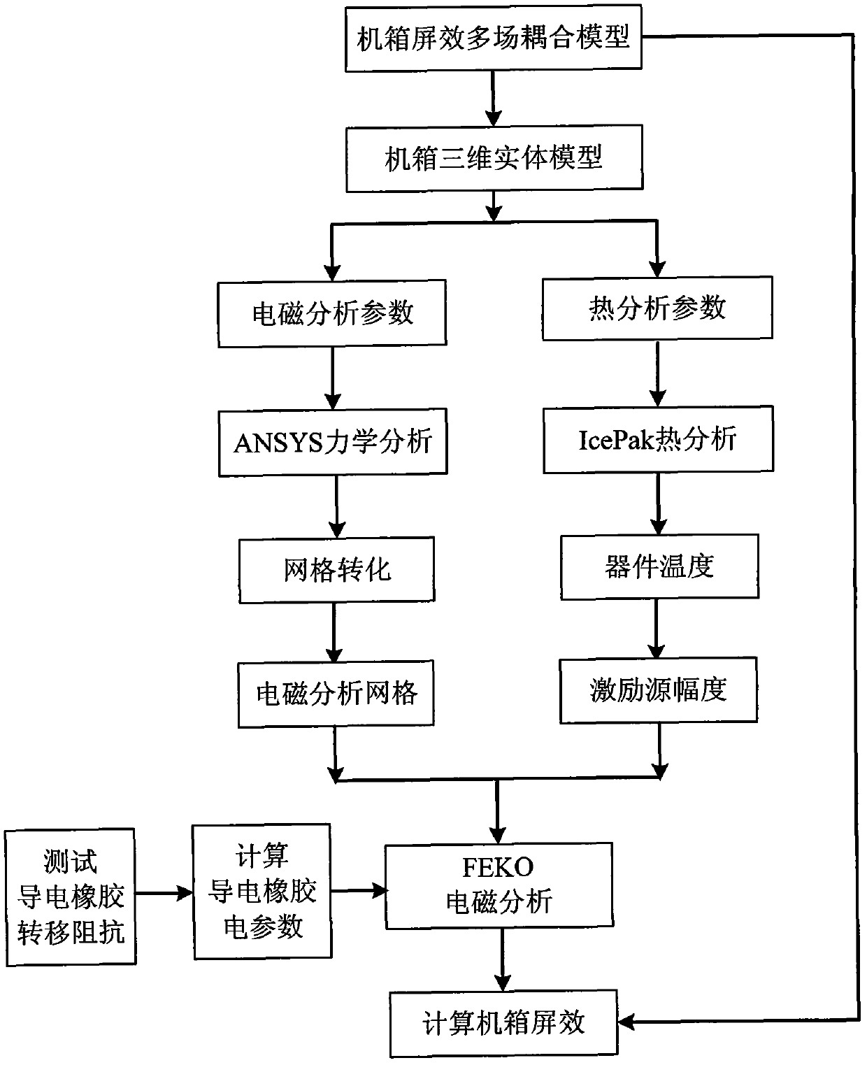
[0036] The present invention will be described in further detail below with reference to the accompanying drawings.

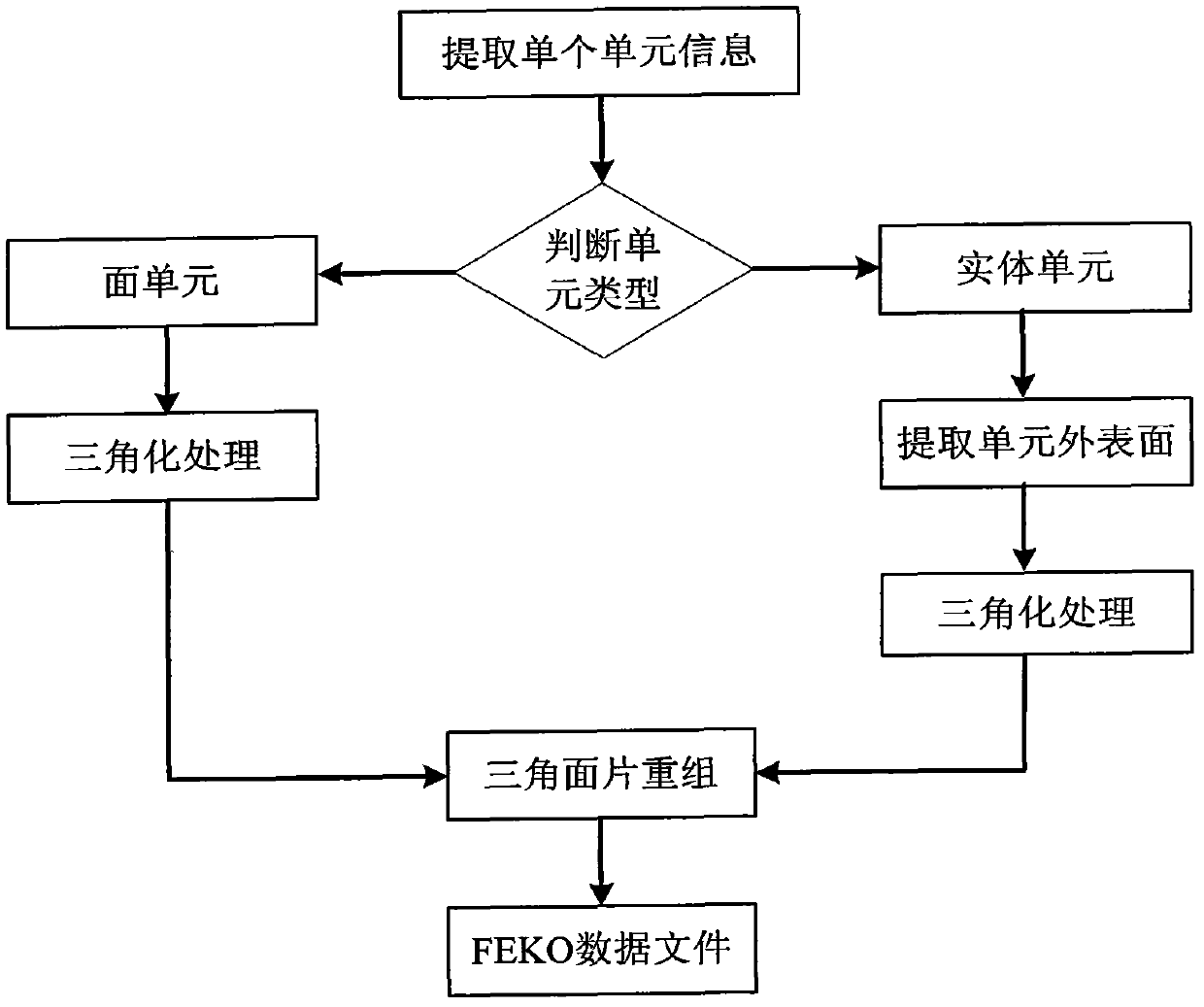
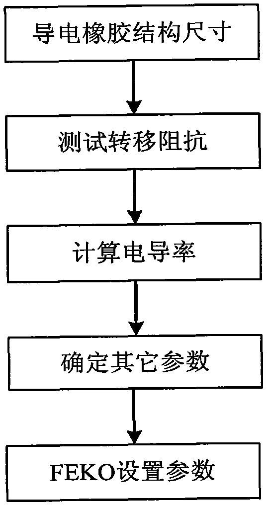
[0037] refer to figure 1 , the concrete steps of the present invention are as follows:

[0038] Step 1: Establish a theoretical model of the electromechanical and thermal three-field coupling of the electromagnetic screen effect of the electronic equipment chassis.

[0039] (1.1) The basic calculation formula of the electromagnetic screen effect of the chassis

[0040] For example Figure 4 As shown in the case of an electronic equipment, suppose there are M electromagnetic devices in it, and the observation point at a distance d from the center of the case is p. The electric field intensity at point P with and without the case is respectively with Define the chassis screen effect as:

[0041] SE = 20 log | Σ i = ...


PUM


Abstract

The invention discloses an electromagnetic shielding effect simulation method for an electronic device chassis with conductive rubber, which is mainly used for solving the problem that the conductive rubber can not be simulated during shielding effect simulation in the prior art. The steps are as follows: establishing a multi-field coupling theoretical model for shielding effect of the chassis; introducing a chassis solid model established by Pro/E (pro/engineer) into Ansys for calculating structural displacement; transforming structural grids to electromagnetic grids and introducing into Feko software; measuring the transfer impedance of the conductive rubber, calculating the electrical conductivity and determining other electrical parameters; introducing the solid model into IcePak, and calculating the temperature of all devices in the chassis; determining the magnitude of a driving source through a curve of a device radiation electric field along with the temperature change according to the temperature; setting the parameters of the conductive rubber and the magnitude of the driving source in the FEKO and calculating the electric field value of an observation point outside the chassis; and putting the electric field value into the multi-field coupling theoretical model and obtaining the shielding effect of the chassis. The electromagnetic shielding effect simulation method can simulate the electromagnetic shielding effect of the electronic device chassis with the conductive rubber, and be used for guiding the design of electromagnetic compatibility of the structure of the chassis.

Description

technical field [0001] The invention belongs to the technical field of electronic equipment and relates to electromagnetic screen effect simulation of a high-density chassis, which can be used to judge whether the electromagnetic screen effect of the chassis meets the design requirements and guide the design of the electronic equipment chassis. Background technique [0002] With the rapid development of radio electronic technology since the middle of the last century, electronic equipment has been widely used in various fields, and the chassis structure has also been widely used as the physical assembly and carrying platform of various components of electronic equipment. The design of modern chassis has electromagnetic compatibility requirements, and the main indicator is the electromagnetic screen effect of the chassis. [0003] Due to the installation of various switches, instrument panels, cables, etc. on the surface of the chassis, there must be holes and seams, which wi...

Claims


Application Information

Patent Timeline
Patent Type & Authority Applications(China)
IPC IPC(8): G06F17/50H05K9/00
Inventor 段宝岩李鹏胡凯博马伯渊徐达人杜敏
Owner XIDIAN UNIV
Why Eureka
Try Eureka