Photolithography equipment vacuum exposure device

A technology of exposure device and lithography machine, which is applied in the field of lithography, can solve the problems of affecting the quality of lithography, poor contact between the mask plate and the silicon wafer, etc., and achieve the effects of increasing exposure, convenient installation and adjustment, and simple mechanism

Inactive Publication Date: 2013-02-20
INST OF OPTICS & ELECTRONICS - CHINESE ACAD OF SCI
View PDF0 Cites 0 Cited by
  • Summary
  • Abstract
  • Description
  • Claims
  • Application Information

AI Technical Summary

Problems solved by technology

[0002] In a close-contact lithography machine, the quality of lithography is greatly affected by the poor contact between the mask and the silicon wafer, and the different degrees of refraction and reflection of the light source due to the other gases filled between them.

Method used


Image

  • Photolithography equipment vacuum exposure device
  • Photolithography equipment vacuum exposure device
  • Photolithography equipment vacuum exposure device

Examples


Embodiment Construction

[0015] In order to make the object, technical solution and advantages of the present invention clearer, the present invention will be described in further detail below in conjunction with specific embodiments and with reference to the accompanying drawings.

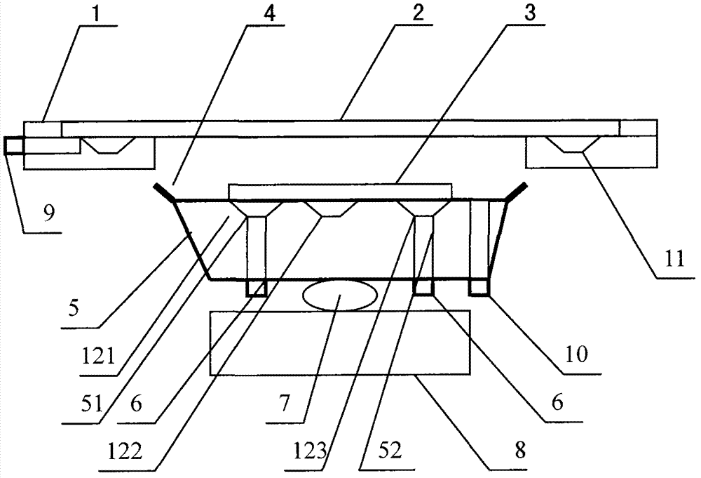
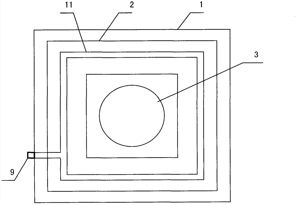
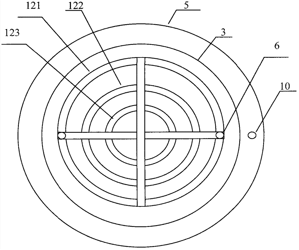
[0016] like figure 1 As shown, the vacuum exposure device of the lithography machine of the present invention includes: a mask table 1, a mask plate 2, a silicon wafer 3, a sealing rubber ring 4, a film receiving table 5, two gas nozzles 6, a flexible hinge 7, an elevating table 8, The first air nozzle 9 and the vacuum air nozzle 10; the mask plate 2 is placed on the mask table 1, the silicon wafer 3 is placed on the wafer table 5, the sealing rubber ring 4 is set on the outside of the wafer table 5, and the wafer table 5 It is connected with the lifting table 8 through a flexible hinge 7; the masking table 1 is located above the film carrier 5, and the masking table 1 is provided with a V-shaped groove 11, and the film c...


PUM


Abstract

The invention relates to a mask aligner vacuum exposure device. The vacuum exposure device comprises a mask platform, a mask plate, a silicon wafer, a rubber seal ring, a wafer carrier, two air taps, a flexible hinge, a lifting table, a first air tap and a vacuum air tap, wherein the mask plate is arranged on the mask platform; the silicon wafer is arranged on the wafer carrier; the rubber seal ring is sleeved on the outside of the wafer carrier; the wafer carrier is connected with the lifting table through the flexible hinge; the mask platform is arranged above the wafer carrier; the mask platform is provided with a V-shaped groove, and the wafer carrier is also provided with a V-shaped groove; and vacuum-pumping operation is performed on the V-shaped groove of the mask platform and the V-shaped groove of the wafer carrier, thus the silicon wafer can contact with the mask plate well. By adopting the mask aligner vacuum exposure device, a silicon wafer to be exposed can be in the vacuum environment, the influences of anaclasis or reflection of other gases on photolithography can be overcome and the photolithography resolution of the silicon wafer can be increased.

Description

technical field [0001] The technical field of photolithography of the present invention relates to a vacuum exposure device of a photolithography machine. Background technique [0002] In a close-contact lithography machine, the quality of lithography is greatly affected by the poor contact between the mask and the silicon wafer, and the different degrees of refraction and reflection of the light source due to the other gases filled between them. . Therefore, it is very necessary to evacuate the gap between the mask plate and the silicon wafer before lithography exposure, which can not only greatly improve the line resolution of lithography, but also improve the quality of lithography. Contents of the invention [0003] In order to solve the problems of the prior art, the object of the present invention is to realize that the mask plate and the silicon wafer are in a vacuum environment state, and to ensure good contact between the mask plate and the silicon wafer. For thi...

Claims


Application Information

Patent Timeline
Patent Type & Authority Patents(China)
IPC IPC(8): G03F7/20
Inventor 邢薇胡松赵立新徐文祥胡淘陈磊
Owner INST OF OPTICS & ELECTRONICS - CHINESE ACAD OF SCI
Why Eureka
Try Eureka