Quick read-write method and device for flash memory

A method of reading and writing, flash memory technology, applied in the direction of memory address/allocation/relocation, etc., can solve the problems of multi-program storage space, occupation, waste of time, etc.

Active Publication Date: 2011-05-25
ZTE INTELLIGENT IOT TECH
View PDF0 Cites 13 Cited by
  • Summary
  • Abstract
  • Description
  • Claims
  • Application Information

AI Technical Summary

Problems solved by technology

Therefore, reading and writing FLASH according to the usual habits will waste a lot of time on erasing and writing operations, and the service life of FLASH will be shortened due to the unbalanced number of times of erasing and writing in different spaces.
[0003] There are relatively mature meth

Method used


Image

  • Quick read-write method and device for flash memory
  • Quick read-write method and device for flash memory
  • Quick read-write method and device for flash memory

Examples


Embodiment Construction

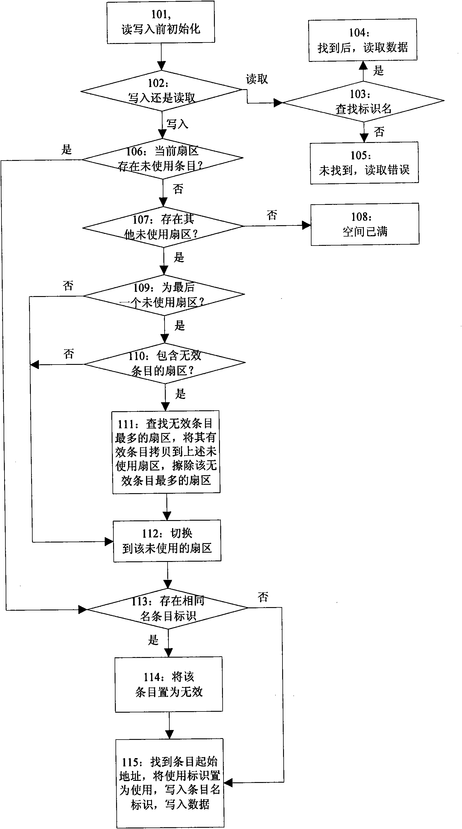
[0018] The core of the present invention lies in: organizing and storing data in the FLASH in the form of fixed-format entries, and reading, writing, erasing and space arrangement are all performed based on entries.

[0019] The interior of FLASH is generally divided into n (n≥2) sectors, and the size of each sector is 2 m Byte and sector are the minimum erasing unit of FLASH. Each sector is also logically divided with a size of 2 j byte entries, each sector can hold 2 k such entries, thus j+k=m.

[0020] The data stored in the entry includes: use identifier, effective identifier, entry name identifier and data information.

[0021] According to this, the data to be read and written can be reasonably divided, and the length of 2 j data block of bytes.

[0022] The FLASH reading and writing method of the present invention organizes and stores data in the FLASH according to the form of fixed-format entries, and the format of the entries is as follows: figure 1 shown.

[0...


PUM


Abstract

The invention discloses a quick read-write method and a quick read-write device for a flash memory. The method comprises the following steps of: dividing entries into each sector in the flash memory, and dividing to-be-written data for storage according to the length of the entries, wherein each entry is used for bearing data; when the data are written, querying the unused entries in the current sector, and writing the data into the unused entries; when only one unused sector is queried, if the entries of invalid data are stored in other sectors is detected, reclaiming the space occupied by the entries; otherwise, directly writing the data into the unused data. The data are organized and stored according to a form of entries of fixed formats. When the data are modified, the original entries are not modified, but the original entries are set to be invalid, and new entries are written, so the erasing frequency is reduced, the average writing speed is quickened, and balanced access of different storage units of the FLASH is ensured.

Description

technical field [0001] The invention relates to the technical field of embedded systems, in particular to a method and device suitable for realizing balanced reading and writing of NOR FLASH in a simple manner. Background technique [0002] FLASH (flash memory) is often used as memory in embedded systems. On the one hand, each FLASH write operation needs to erase the corresponding position; Take time. Therefore, reading and writing FLASH according to the usual habit will waste a lot of time on erasing and writing operations, and the service life of FLASH will be shortened due to the unbalanced number of times of erasing and writing in different spaces. [0003] There are relatively mature methods for accessing FLASH, but they all use complex algorithms, which require more program storage space and CPU running time to implement. For the case of using a low-performance CPU, the above method is not applicable, and a relatively simple and fast method needs to be found to meet ...

Claims


Application Information

Patent Timeline
IPC IPC(8): G06F12/02
Inventor 付忠鑫徐运张恺
Owner ZTE INTELLIGENT IOT TECH
Why Eureka
Try Eureka