MEMS (micro electro mechanical system) device and wafer-level vacuum packaging method thereof

A technology of devices and silicon wafers, which is applied in the field of MEMS devices and wafer-level vacuum packaging of MEMS devices, can solve the problems of complex process, high cost, and short vacuum holding time, and achieve simple process, reliable performance, and long vacuum holding time. Effect

Active Publication Date: 2014-08-13
EAST CHINA INST OF OPTOELECTRONICS INTEGRATEDDEVICE
View PDF6 Cites 0 Cited by
  • Summary
  • Abstract
  • Description
  • Claims
  • Application Information

AI Technical Summary

Problems solved by technology

In addition, the glass-silicon bonded silicon process is used to carry out wafer-level vacuum packaging of MEMS devices. It mainly adopts the packaging structure method of punching lead through holes on the back of the substrate glass, but the process is complicated, high in cost, and short in vacuum holding time.

Method used


Image

  • MEMS (micro electro mechanical system) device and wafer-level vacuum packaging method thereof
  • MEMS (micro electro mechanical system) device and wafer-level vacuum packaging method thereof
  • MEMS (micro electro mechanical system) device and wafer-level vacuum packaging method thereof

Examples


Embodiment Construction

[0031] 1. The structure of MEMS devices:

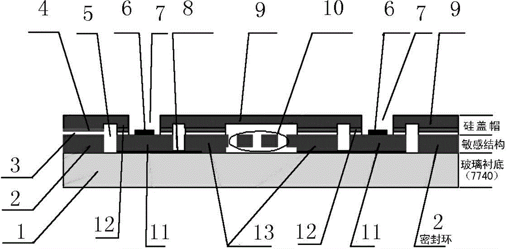
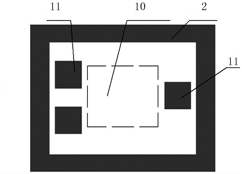
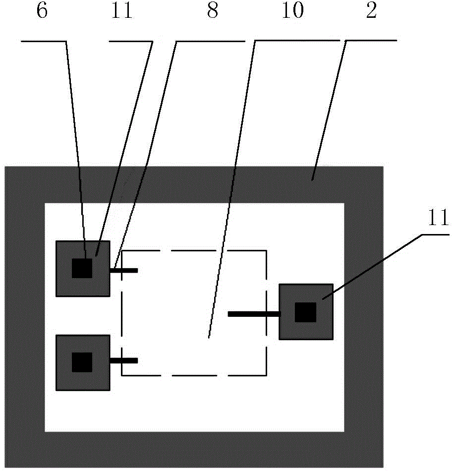
[0032] See attached figure 1 , a MEMS device provided by the present invention, a group of MEMS devices are produced on a silicon wafer, and each MEMS device is composed of a glass substrate 1, a silicon chip sensitive structure layer with a sealing ring 2 and a silicon cap 9.

[0033] Three silicon islands 11 are arranged in the sensitive structure layer of the silicon chip (silicon islands are set according to the number and position of the bonding pads, and the present embodiment is designed as three silicon islands), and each silicon island 11 is isolated from other components of the sensitive structure layer. Insulation, the bottom of each silicon island 11 is respectively connected to the glass substrate 1 and an electrode lead 8 arranged on the glass substrate, each silicon island 11 is respectively provided with a bonding point 6; the silicon cap is connected to each silicon island The corresponding positions are respectively...


PUM


Abstract

A MEMS device and wafer-level vacuum packaging method thereof, consisting of a glass substrate (1), a silicon wafer sensitive structure layer with a sealing ring (2) and a silicon cap (9), characterized in that: the silicon wafer sensitive structure At least two silicon islands (11) are arranged in the layer, and the bottom of each silicon island (11) is connected with the glass substrate (1) and the electrode leads (8), and each silicon island (11) is respectively provided with pressure welding point (6); the corresponding position of each silicon island on the silicon cap is respectively provided with a bonding point cavity (7), so that the bonding point (6) is in the bonding point cavity (7), and the bonding point cavity (7) A pressure welding point sealing ring (12) is provided on the periphery of the cavity to connect and cooperate with the upper surface of the silicon island, and a pressure welding point isolation groove (5) is provided on the periphery of the pressure welding point sealing ring. The invention has the advantages of avoiding the electrical isolation technical problem between the sealing structure of the pressure welding point and the pressure welding point when the electrode is introduced from the base substrate to the surface of the device structure layer. The vacuum packaging structure of the present invention is reasonable in design, simple in process, long in vacuum holding time, reliable in performance and versatile, and reduces the cost of vacuum packaging.

Description

technical field [0001] The invention belongs to the field of micro-electromechanical technology, and relates to a MEMS device and a wafer-level vacuum packaging method for the MEMS device. Background technique [0002] MEMS (abbreviation for Micro Electro Mechanical systems, Micro Electro Mechanical Systems) devices usually contain some movable parts, these movable parts are very fragile, and are easily affected by factors such as dust and water vapor in the process of dicing and assembly, causing damage to the device Or the decline of the overall performance. At the same time, many MEMS devices need to work in a vacuum environment to reduce air damping and improve the quality factor Q value of the device. Such as MEMS accelerometers, micro gyroscopes, micro resonators, thin film pressure sensors, radio frequency MEMS components, vacuum field emitters and some optical MEMS devices, etc. The quality of vacuum packaging directly determines the performance of such devices, so ...

Claims


Application Information

Patent Timeline
Patent Type & Authority Patents(China)
IPC IPC(8): B81B7/02B81B3/00B81C1/00
Inventor 方澍郭群英徐栋黄斌陈博
Owner EAST CHINA INST OF OPTOELECTRONICS INTEGRATEDDEVICE
Why Eureka
Try Eureka