Method and system for realizing bus connection

A bus and extended interface technology, applied in the field of bus connection, can solve the problems of high operating frequency, large delay, and timing that cannot meet the requirements of high-frequency operation, so as to avoid timing problems, ensure timing optimization, and achieve correct interaction. Effect

Inactive Publication Date: 2011-06-22
ZTE CORP +1
View PDF0 Cites 14 Cited by
  • Summary
  • Abstract
  • Description
  • Claims
  • Application Information

AI Technical Summary

Problems solved by technology

However, sometimes it is necessary to use an AXI bus to connect between chips or between a chip and a field-programmable gate array (Field-Programmable Gate Array, FPGA). The delay of the PAD itself is relatively large. In this case, when the AXI bus is used to connect, the operating frequency cannot be very high, and the timing cannot meet the requirements of high-frequency operation.

Method used


Image

  • Method and system for realizing bus connection
  • Method and system for realizing bus connection
  • Method and system for realizing bus connection

Examples


Embodiment Construction

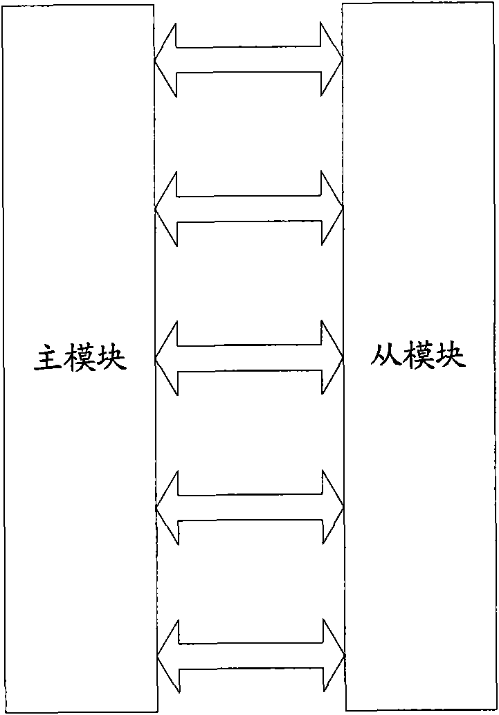
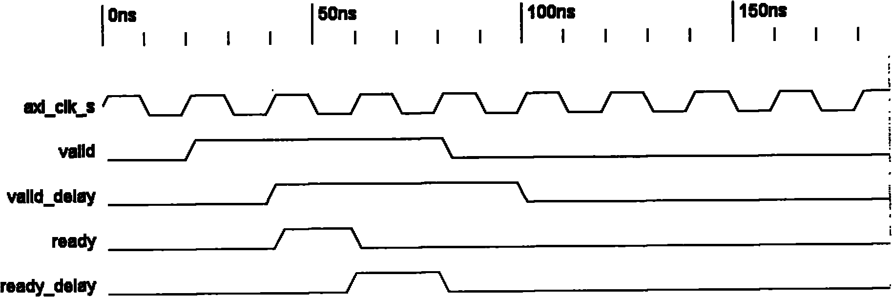
[0049] The specific implementation manners of the present invention will be described in detail below in conjunction with the accompanying drawings. figure 1 Shown is the existing AXI bus connection. Its master module (AXI MASTER) and slave module (AXI SLAVE) are directly connected, in this connection situation. If two chips or two FPGAs and an AXI bus are needed to connect between the chips and the FPGA, the delay of the PAD and the wiring may add up to a delay of more than one cycle. If the timing path between the master and slave blocks exceeds one cycle, a figure 2 error conditions that occur in . Due to the delay of more than one cycle on the connection, the valid valid signal on the master module side is sent out in the first cycle, and it will not be collected until the second cycle on the slave module side. The valid valid signal is received from the module side, the ready signal is set high, and then fed back to the main module side, it takes the third cycle to be...


PUM


Abstract

The invention discloses a method and a system for realizing bus connection. The method comprises the following steps that: a main module buffer receives a transmission request, initiated by a main module, of an advanced expandable interface bus; the main module buffer writes information according to the transmission request; when the main module buffer has the information, the main module buffer transmits the information to a slave module buffer; and the information is transmitted buffer to a slave module by the slave module. By the method and the system for realizing the bus connection, which is provided by the invention, as the main module buffer and the slave module buffer are adopted between the main module and the slave module, the signal input / output between the main module and the slave module is connected with a register, and the time sequence optimization of the bus connection can be guaranteed to the maximum extent.

Description

technical field [0001] The invention relates to a method and system for realizing bus connection. Background technique [0002] With the development of integration technology and the continuous expansion of application fields, different types of integrated circuits are embedded with each other, forming various embedded systems (Embedded System, ES) and systems on a chip (System On Chip, SOC). Among them, SOC refers to the technology of integrating a complete system on a single chip and grouping all or part of the necessary electronic circuits. The so-called complete system generally includes a central processing unit (CPU), memory, and peripheral circuits. [0003] The interconnection between SOCs also has relatively high requirements for the bus. Since the Advanced eXtensible Interface (AXI) bus is an advanced bus interconnection technology with very high efficiency of separating read and write, and separating addresses and data, therefore, Generally, the interconnection ...

Claims


Application Information

Patent Timeline
IPC IPC(8): G06F13/40
Inventor 方应龙曾代兵林晓涛
Owner ZTE CORP
Why Eureka
Try Eureka