Eureka AIR delivers breakthrough ideas for toughest innovation challenges, trusted by R&D personnel around the world.

Resistance-type touch screen

A resistive touch screen technology, applied in electrical digital data processing, instruments, calculations, etc., can solve problems such as damage to the resistance of the upper conductive film layer, affect the function of the touch screen, and sag, so as to suppress the sag and avoid poor function of the touch screen. The effect of reducing the chance of damage

Inactive Publication Date: 2011-06-29
BYD CO LTD
View PDF5 Cites 2 Cited by
  • Summary
  • Abstract
  • Description
  • Claims
  • Application Information

AI Technical Summary

Problems solved by technology

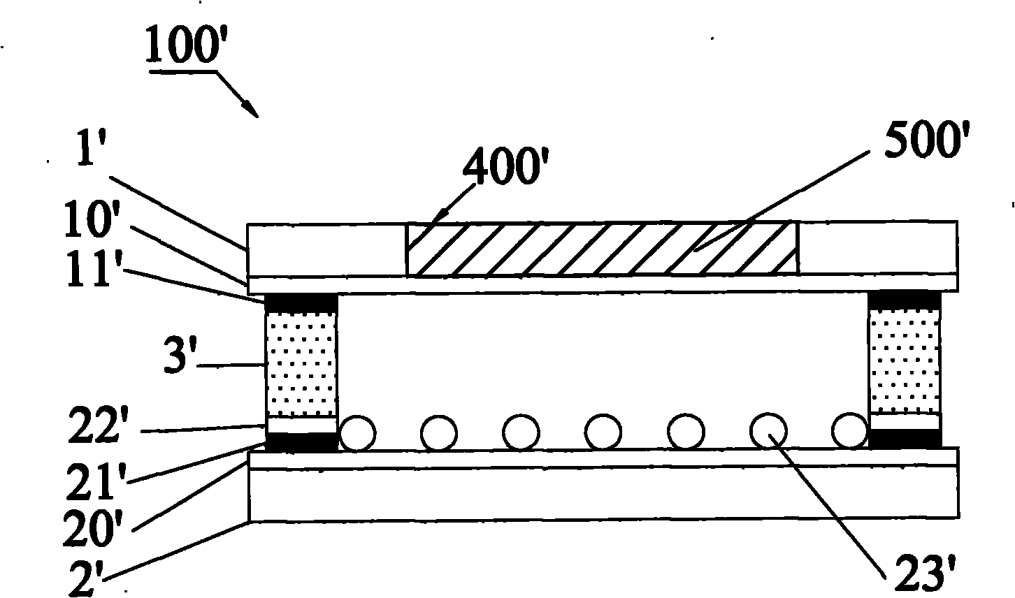
[0004] The present invention aims to solve the defect that the edge of the upper substrate of the existing resistive touch screen tends to sag toward the lower substrate under long-term stress, thereby causing damage to the resistance of the upper conductive film layer and further affecting the function of the touch screen. An Improved Resistive Touch Screen

Method used


Image

  • Resistance-type touch screen
  • Resistance-type touch screen
  • Resistance-type touch screen

Examples


Embodiment Construction

[0014] In order to make the technical problems, technical solutions and beneficial effects solved by the present invention clearer, the present invention will be further described in detail below in conjunction with the accompanying drawings and embodiments. It should be understood that the specific embodiments described here are only used to explain the present invention, not to limit the present invention.

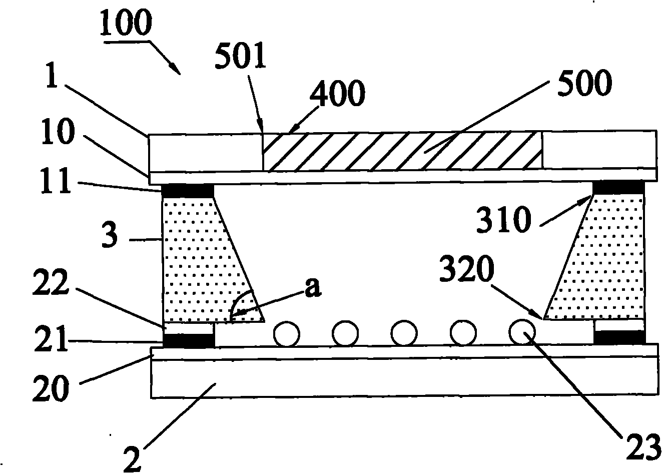
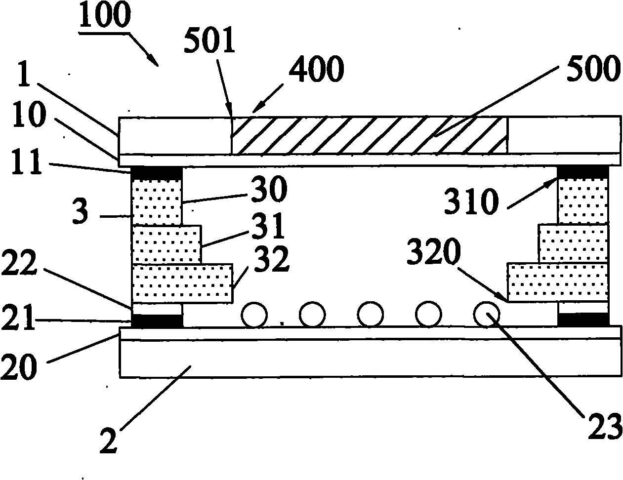
[0015] Such as figure 2 as well as image 3 As shown, a resistive touch screen 100 provided by the present invention includes an upper substrate 1, an upper conductive layer 10 disposed on the upper substrate 1, an upper electrode 11 formed on the edge of the upper conductive layer 10, and the upper substrate 1 The lower substrate 2 oppositely arranged, the lower conductive layer 20 arranged on the lower substrate 2 and opposite to the upper conductive layer 10, the lower electrode 21 formed on the edge of the lower conductive layer 20, and the lower electrode 21 arran...


PUM

PropertyMeasurementUnit
Angleaaaaaaaaaa
Angleaaaaaaaaaa
Thicknessaaaaaaaaaa

Abstract

The invention provides a resistance-type touch screen, which includes an upper substrate, an upper conducting layer arranged on the upper substrate, an upper electrode formed on the edge of the upper conducting layer, a lower substrate arranged opposite to the upper substrate, a lower conducting layer arranged on the lower substrate and opposite to the upper conducting layer, a lower electrode formed on the edge of the lower conducting layer, and a bonding layer arranged between the upper conducting layer and the lower conducting layer, wherein the transverse length of a first edge when the bonding layer is in contact with the lower conducting layer is larger than that of a second edge when the bonding layer is in contact with the upper conducting layer. The invention can prevent the upper substrate from being in complete contact with the lower substrate provided with the lower conducting layer, and restrain the depressed degree of the upper substrate to a certain extent, thereby reducing the damage possibility of the upper conducting layer on the upper substrate and further preventing the problem of poor function of the touch screen which is caused by the damage on the resistance uniformity of the upper conducting layer on the upper edge of the upper substrate.

Description

technical field [0001] The invention belongs to the field of touch screens, in particular to a resistive touch screen. Background technique [0002] Such as figure 1 As shown, the structure of the resistive touch screen 100' in the prior art includes: an upper substrate 1', an upper conductive thin film layer 10' and an upper electrode 11' sequentially arranged on the upper substrate 1', a lower substrate 2', and an opposite The upper substrate 1' is arranged on the lower conductive film layer 20', the lower electrode 21', the insulating layer 22' and the isolation dot array layer 23' on the lower substrate 2', and the upper substrate 1' and the lower substrate 2 'By double sided tape 3' glued together and sealed. It can be seen from the figure that there is a drawing area 500' on the upper substrate 1' of the resistive touch screen 100', and there is a bending area 400' at 1 mm from the edge of the drawing area 500'. [0003] In the structure of the above-mentioned resis...

Claims


Application Information

Patent Timeline
IPC IPC(8): G06F3/045
Inventor 张帆李生林
Owner BYD CO LTD
Why Eureka
Eureka Blog
Learn More