Semiconductor component test station with detachable electric property detecting system

A detection system and semiconductor technology, which is applied to the testing of single semiconductor devices, components of electrical measuring instruments, and electrical measurement, etc., can solve the problems of surface scratches, defect rate, cost, and contamination of the components to be tested, and achieve operational flexibility. Increase, reduce the damage probability, improve the effect of detection efficiency

Inactive Publication Date: 2008-12-03
CHROMA ATE
View PDF0 Cites 16 Cited by
  • Summary
  • Abstract
  • Description
  • Claims
  • Application Information

AI Technical Summary

Problems solved by technology

[0016] In this way, although the unnecessary downtime of the machine and the cost of human resource processing can be reduced, on the one hand, the component to be tested has been sucked and moved multiple times in each step of the two sets of test equipment. Scratches and stains on the surface of the test component; and the highest requirements on surface integrity and cleanliness, such as photosensitive component CMOS, etc., which means increasing the defect rate and cost

Method used


Image

  • Semiconductor component test station with detachable electric property detecting system
  • Semiconductor component test station with detachable electric property detecting system
  • Semiconductor component test station with detachable electric property detecting system

Examples


Embodiment Construction

[0045] The foregoing and other technical contents, features and effects of the present invention will be clearly presented in the following detailed description of preferred embodiments with reference to the accompanying drawings.

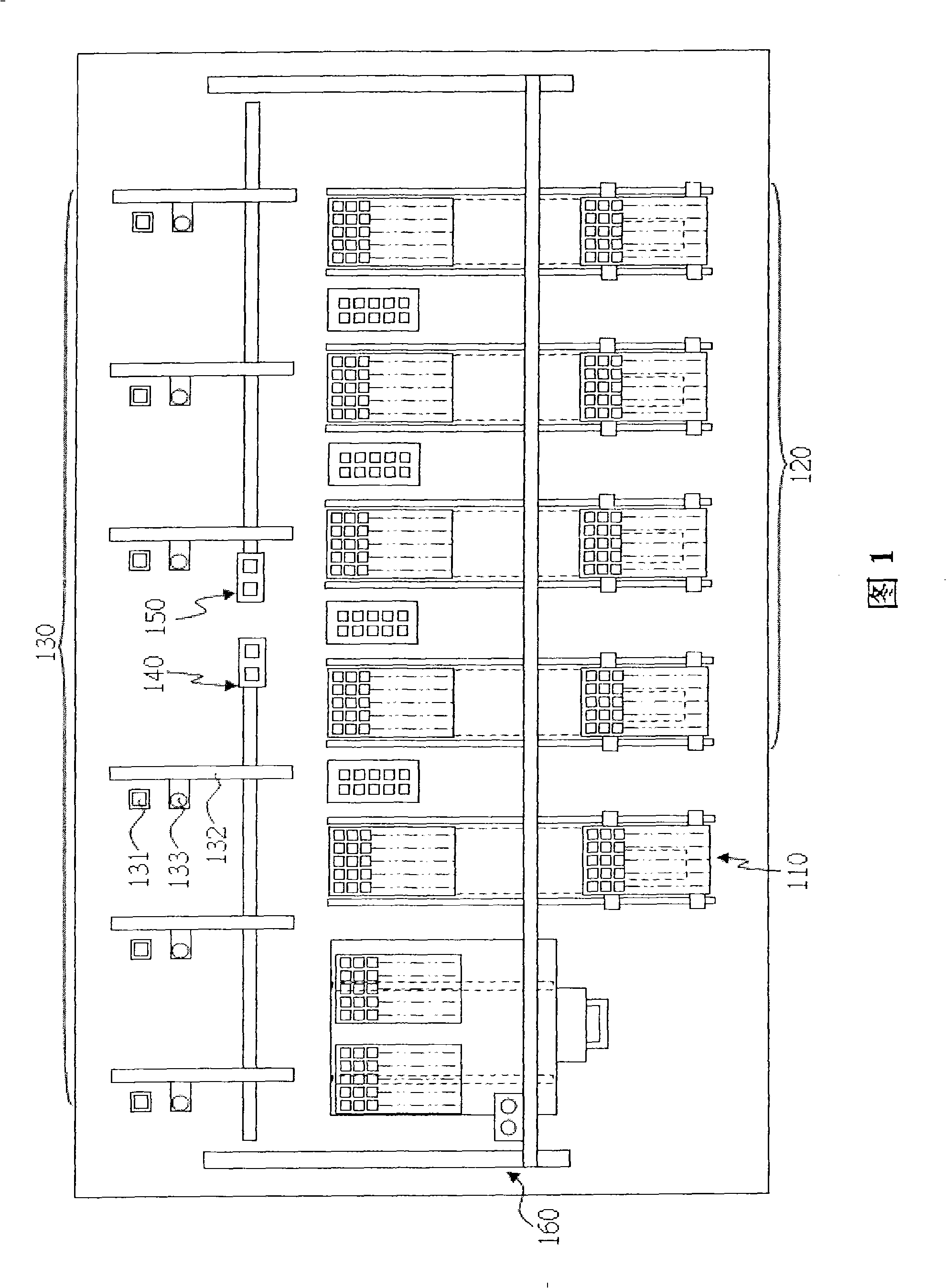
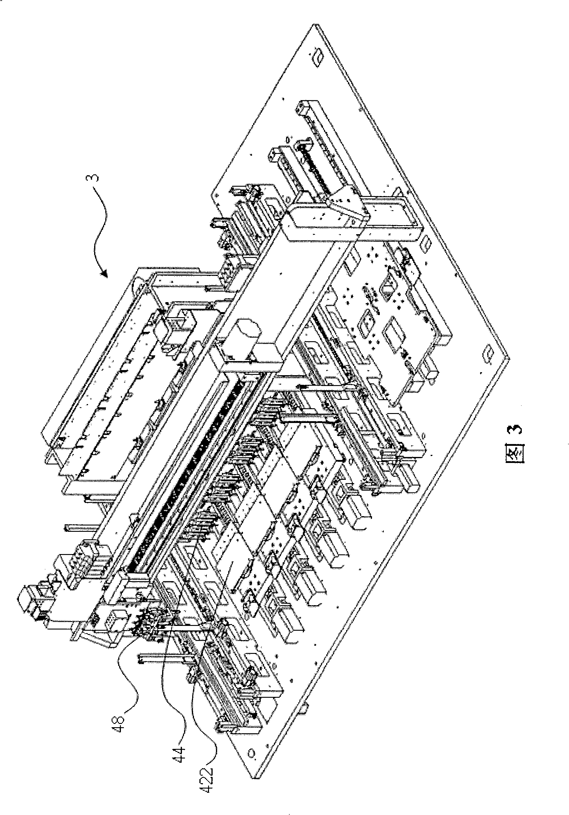
[0046] A preferred embodiment of a semiconductor component testing machine with a separable electrical testing system according to the present invention. FIG. 3 is a three-dimensional schematic view of the appearance of the machine 3; FIG. In this embodiment, a test machine with four sets of test areas is taken as an example, and each test area can test 4 semiconductor components to be tested at a time, so each batch can be 4×4=16 semiconductor components to be tested are tested, thus having a high test efficiency.

[0047] The machine 3 includes: an actual testing system 4 , an electrical testing system 40 , and a control device 47 . In this example, the real-world testing system 4 includes: a plurality of sets of correspondingly configured test ...


PUM


Abstract

The invention relates to a semiconductor component testing machine with a separable electrical detection system. After the semiconductor component to be tested is viewed for correct arrangement, the semiconductor component to be tested is moved to the position to be tested, and electrically connected to the electrical detection system for performing electrical detection through the switching of a connector, thereby carrying out a continuous detection procedure for efficiency detection by switching at the original testing position. The testing procedures are consecutive, the time of absorbing and moving the component to be tested is reduced, the damage probability of the component to be tested is reduced, and the detection efficiency and the proper handling rate of the tested component are improved. Two systems can be separated according to the requirement, and the efficiency detection procedure of the semiconductor component to be tested is respectively performed, thereby avoiding the pointless increase of the machine cost and improving the use elasticity.

Description

【Technical field】 [0001] The invention relates to a semiconductor component testing machine, in particular to a semiconductor component testing machine with a separable electric property detection system. 【Background technique】 [0002] Semiconductor components have become the indispensable core of most electronic equipment, and are widely used in the daily life of the general public, such as microprocessors in various electrical appliances and household appliances, CMOS (Complementary Metal-Oxide Semiconductor, complementary metal oxide semiconductor), etc., the reliability of semiconductor components has undoubtedly become an important key to determine the reliability of electronic equipment. [0003] At present, the automated testing machines used to test semiconductor components can be roughly divided into analog tests that provide analog signals from the test base and capture the output signals of each output pin to find open circuit, short circuit or misconnection of t...

Claims


Application Information

Patent Timeline
Patent Type & Authority Applications(China)
IPC IPC(8): G01R31/26G01R1/02
Inventor 许良宇
Owner CHROMA ATE
Why Eureka
Try Eureka