Supercharge Your Innovation With Domain-Expert AI Agents!

Semiconductor memory device

A semiconductor and memory technology, which is applied in the field of semiconductor memory devices and can solve the problems of reducing the response speed of data writing requests and the like

Active Publication Date: 2011-08-24
키오시아가부시키가이샤
View PDF8 Cites 6 Cited by
  • Summary
  • Abstract
  • Description
  • Claims
  • Application Information

AI Technical Summary

Problems solved by technology

However, when compressed, the bandwidth of NAND memory is squeezed due to the reading and writing of valid data, which results in a significant slowdown in the response speed to data write requests from the host

Method used


Image

  • Semiconductor memory device
  • Semiconductor memory device
  • Semiconductor memory device

Examples


Embodiment Construction

[0022] Exemplary embodiments of semiconductor memory devices will be described in detail below with reference to the accompanying drawings.

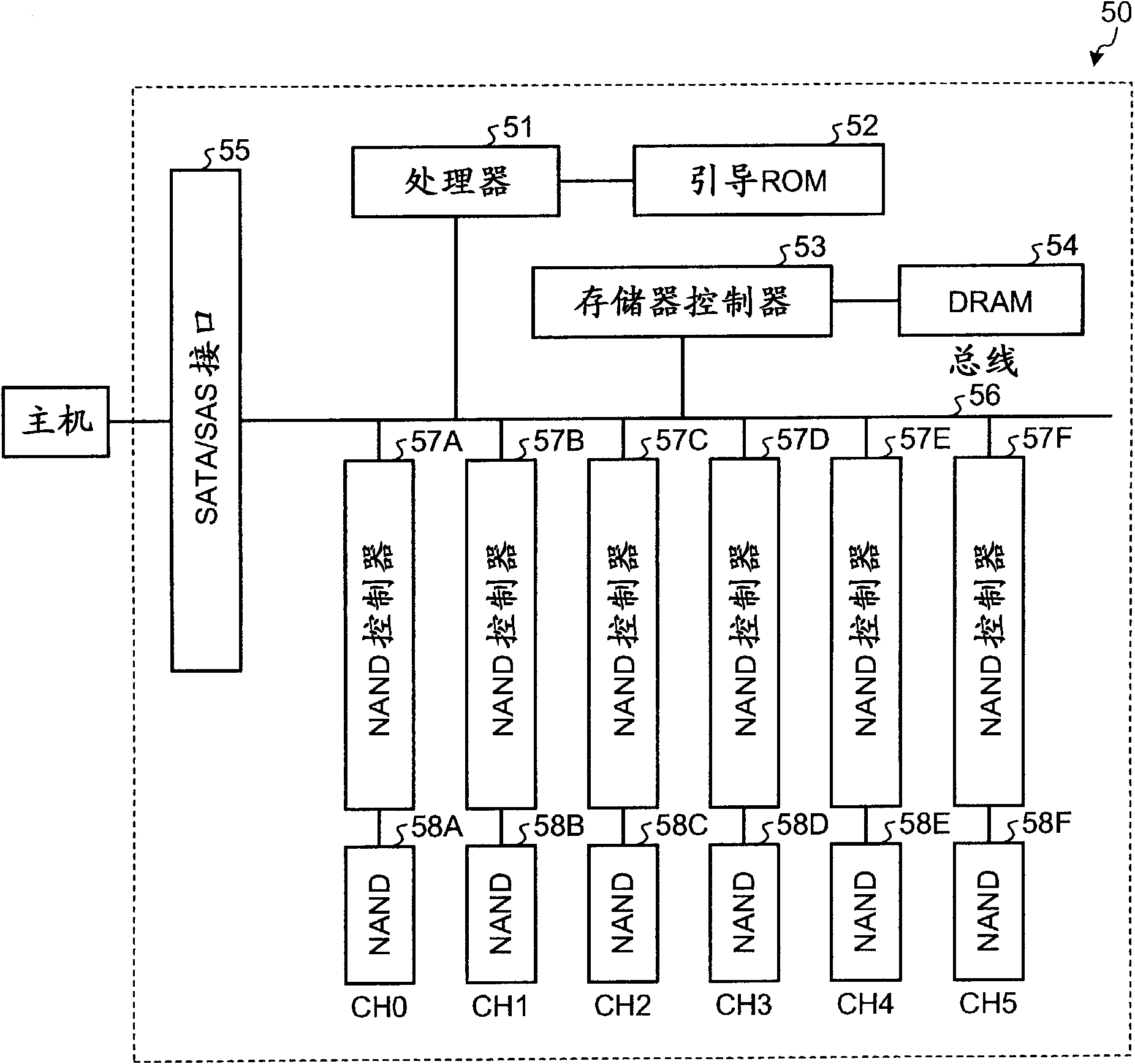
[0023] First, will use figure 1 The hardware configuration of the semiconductor memory device according to the embodiment is described. The semiconductor memory device 50 includes a processor 51, a boot read only memory (boot ROM) 52, a SATA / SAS interface 55, a memory controller 53, a dynamic random access memory (DRAM) 54, NAND controllers 57A to 57F, semiconductor memory elements (NAND) 58A to 58F, and a bus 56 connecting these components. When it is not necessary to distinguish each of the NAND controllers 57A to 57F, the NAND controllers 57A to 57F may be simply referred to as the NAND controller 57 . Similarly, when it is not necessary to distinguish each of the semiconductor memory elements 58A to 58F, the semiconductor memory elements 58A to 58F may be simply referred to as semiconductor memory elements 58 .

[0024] Under the ...


PUM


Abstract

The invention relates to a semiconductor memory device. According to one embodiment, a semiconductor memory device performs writing of data to a semiconductor memory element in response to a request to write the data with a specified logical block address from a host and performs writing of valid data to the semiconductor memory element for compaction according to a log-structured method. The semiconductor memory device adjusts a frequency of the writing response to a request from the host and a frequency of the writing for compaction according to a predetermined ratio.

Description

[0001] Cross References to Related Applications [0002] This application is based on and claims the benefit of priority from Japanese Patent Application No. 2010-031797 filed on February 16, 2010 and Japanese Patent Application No. 2010-206116 filed on September 14, 2010, the entire contents of which are hereby incorporated by reference. technical field [0003] Embodiments described herein relate generally to semiconductor memory devices. Background technique [0004] Due to the increase in capacity of a NAND type flash memory (referred to as NAND memory), which is one type of semiconductor memory chips, semiconductor memory devices using semiconductor memory chips are widely used in recent years. When writing to NAND memory, the NAND memory needs to be erased before writing. Erasing of the NAND memory is performed in blocks such as 512KB in units. This is significantly larger than 4KB, which is a data size more frequently used when writing in response to a request from ...

Claims


Application Information

Patent Timeline
IPC IPC(8): G06F13/16G06F12/02
CPCG06F12/0246G06F2212/7205G11C16/10G11C16/16G11C16/06
Inventor 浅野滋博吉井谦一郎福富和弘菅野伸一
Owner 키오시아가부시키가이샤
Features
  • R&D
  • Intellectual Property
  • Life Sciences
  • Materials
  • Tech Scout
  • Unparalleled Data Quality
  • Higher Quality Content
  • 60% Fewer Hallucinations
Learn More