Method for operating buffer cache of storage device including flash memory

a storage device and buffer cache technology, applied in the field of buffer cache, can solve problems such as reducing the performance of storage devices, and achieve the effect of efficient operation of dram buffer caches

Inactive Publication Date: 2008-08-14
SAMSUNG ELECTRONICS CO LTD
View PDF6 Cites 95 Cited by
  • Summary
  • Abstract
  • Description
  • Claims
  • Application Information

AI Technical Summary

Benefits of technology

[0016]Exemplary embodiments of the present invention provide a method of efficiently operating a DRAM buffer cache of a storage device including a flash memory.

Problems solved by technology

However, a long time is required to search the DRAM buffer cache and this delay can reduce the performance of the storage device.

Method used


Image

  • Method for operating buffer cache of storage device including flash memory
  • Method for operating buffer cache of storage device including flash memory
  • Method for operating buffer cache of storage device including flash memory

Examples


Embodiment Construction

[0049]The above and other features and aspects of the exemplary embodiments of the present invention will be described in detail with reference to the accompanying drawings, in which:

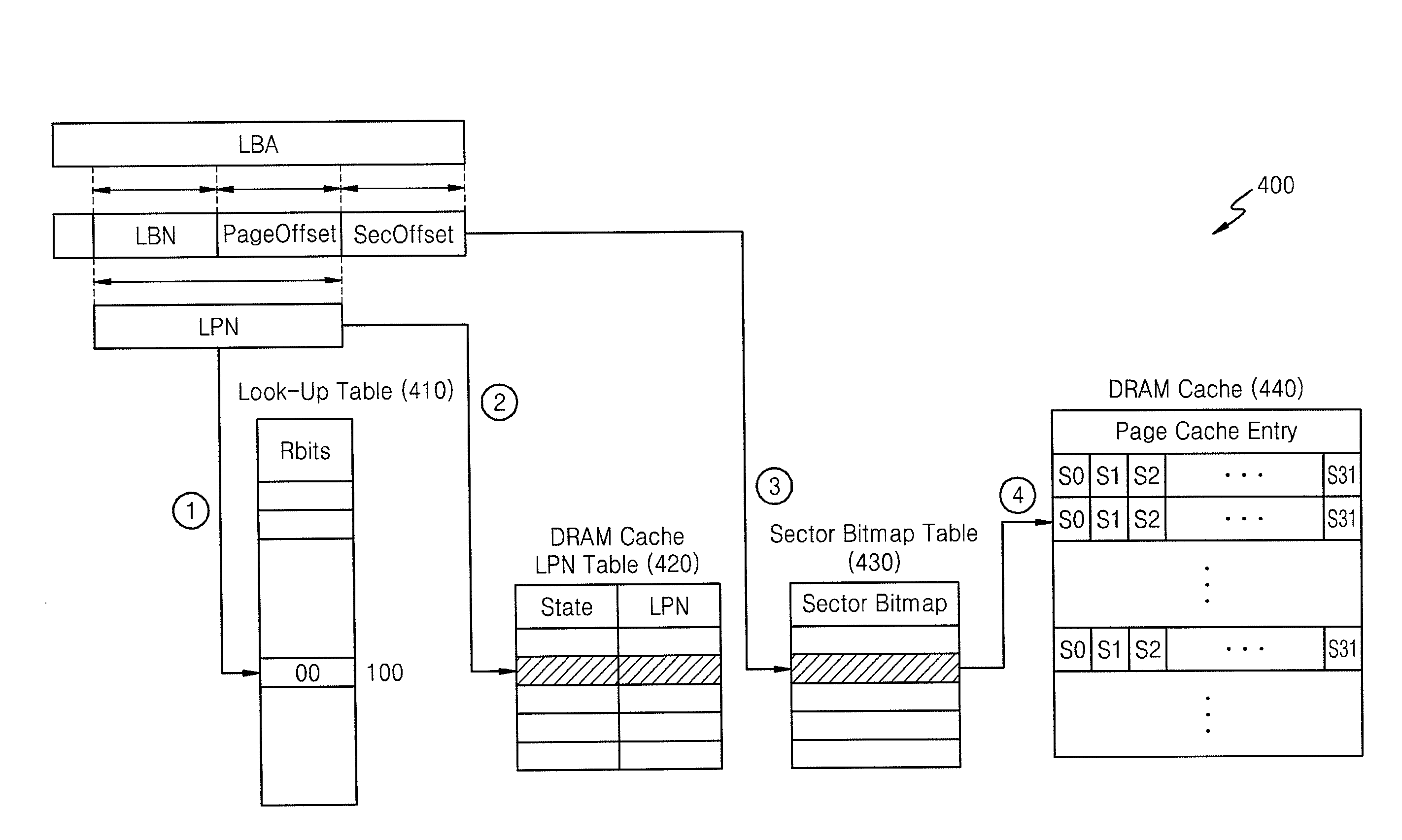
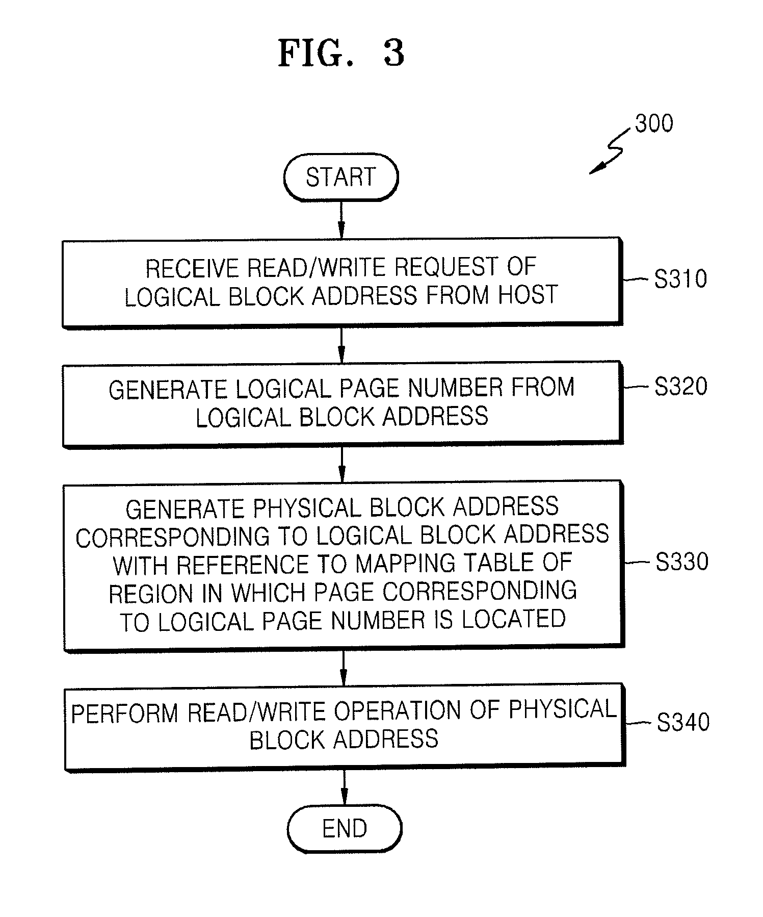
[0050]FIG. 3 is a flowchart showing a read / write method 300 which is performed by a storage device including a flash memory, according to an embodiment of the present invention. The storage apparatus includes a NAND flash memory and a DRAM buffer cache as a buffer cache.

[0051]Referring to FIG. 3, in the read / write method 300, the storage device receives a read / write request for a logical block address from a host (step S310). The host can receive or transmit data from or to the storage device through an Advanced Technology Attachment (ATA) or Serial Advanced Technology Attachment (ATAT) interface.

[0052]If the storage device receives a logical block address LBA, the storage device converts the logical block address LBA into a logical page number (step S320). Then, the storage device generates a physical ...


PUM


Abstract

Provided is a method for operating a buffer cache which is performed by a storage device including a flash memory. The method includes converting a logical block address requested from a host into a logical page number. A region in which a page corresponding to the logical page number is located is searched for. A physical block address corresponding to the logical block address is generated with reference to a mapping table of the region in which the page corresponding to the logical page number is located. The searching for of the region includes searching for a look-up table having information about a region in which a plurality of pages of the flash memory are located.

Description

CROSS-REFERENCE TO RELATED PATENT APPLICATION[0001]This application claims priority to Korean Patent Application No. 10-2007-0015089, filed on Feb. 13, 2007, in the Korean Intellectual Property Office, the disclosure of which is incorporated herein in its entirety by reference.BACKGROUND OF THE INVENTION[0002]1. Technical Field[0003]The present invention relates to a buffer cache, and more particularly, to a method of operating a buffer cache of a storage device including a flash memory.[0004]2. Discussion of the Related Art[0005]Application storage devices, including flash memory, are being developed to quickly operate semiconductor devices. Such application storage devices include Solid State Disks (SSDs), Hybrid Hard Disk Drives (HDDs), etc.[0006]FIG. 1 is a block diagram illustrating the system hardware structure of a SSD.[0007]Referring to FIG. 1, the SSD, which is one type of application storage devices, can use flash and other forms of memory, as buffer cache memory. The SSD ...

Claims


Application Information

Patent Timeline
Patent Type & Authority Applications(United States)
IPC IPC(8): G06F12/02
CPCG06F12/0246G06F2212/7201G06F2212/214G06F12/0866G11C16/06
Inventor CHEON, WON-MOONPARK, CHAN-IK
Owner SAMSUNG ELECTRONICS CO LTD
Why Eureka
Try Eureka