Decoder, data driver and display device

A decoder and digital signal technology, applied in the direction of instruments, static indicators, etc., can solve the problems of increased manufacturing costs, increased masks, increased manufacturing steps, etc., to reduce the area, reduce the gate size, and expand the voltage range Effect

Active Publication Date: 2015-04-29
RENESAS ELECTRONICS CORP
View PDF7 Cites 0 Cited by
  • Summary
  • Abstract
  • Description
  • Claims
  • Application Information

AI Technical Summary

Problems solved by technology

Therefore, the manufacturing cost increases due to an increase in masks, an increase in manufacturing steps, etc.
Furthermore, when the voltage range for lowering Vth is changed, the optimum value of Vth control also changes, and it is not practical to adjust the threshold voltage Vth of the transistor in the manufacturing process according to the condition of the variable voltage range.

Method used


Image

  • Decoder, data driver and display device
  • Decoder, data driver and display device
  • Decoder, data driver and display device

Examples


Embodiment approach 1

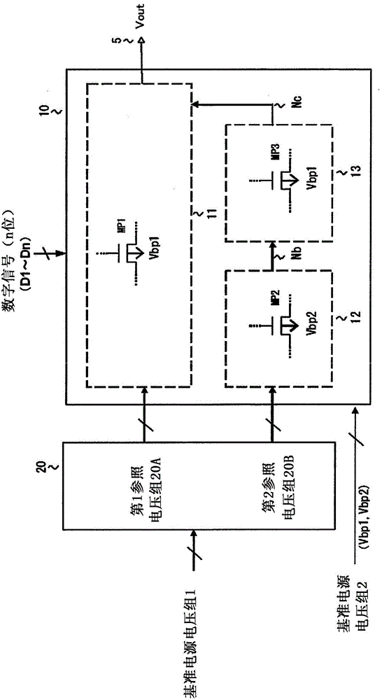
[0055] figure 1 It is a figure which shows the structure of one Embodiment of this invention. figure 1 and Figure 19 The constitution of the decoder of the pMOS transistor is also exemplified. The decoder 10 selects one of the reference voltages from the reference voltage generating circuit 20 according to an n-bit input digital signal (where n is an integer greater than or equal to 2), and outputs it from the terminal 5 . exist figure 1 Among them, as n-bit input digital signals, D1˜Dn and their complementary signals D1B˜DnB are input into the decoder 10 . Wherein, the High potential of the input digital signal is, for example, the high-order power supply voltage VDD, and the Low potential is, for example, the low-order power supply voltage VSS. like figure 1 As shown, the reference voltage generation circuit 20 divides the plurality of reference voltages generated based on the reference power supply voltage group 1 into a first reference voltage group 20A on the hig...

Embodiment 1

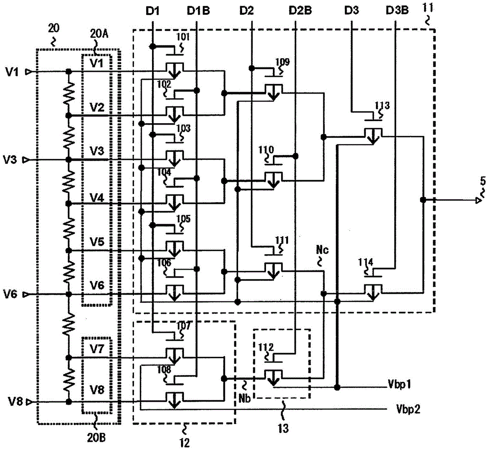
[0062] figure 2 It is a figure which shows the structure of the 1st Example of this invention. exist figure 2 in, as figure 1 A specific example of figure 1 An example of the configuration of the reference voltage generating circuit 20 and the decoding circuit 10. exist figure 2 In the reference voltage generation circuit 20, V1, V3, V6, and V8 are received as the reference power supply voltage group 1, and the label of the voltage dividing resistor (ladder resistor) connected between V1 and V8 is used as the first reference on the high potential side. The voltage group 20A outputs V1, V2, V3, V4, V5, and V6, and the second reference voltage group 20B on the low potential side outputs V7, V8.

[0063] take over figure 1 The 3-bit digital signal (D1, D2, D3) and the complementary signal (D1B, D2B, D3B) of the n-bit digital signal where n is 3 (High potential is the high-side power supply voltage VDD, and the Low potential is the low-side power supply voltage VSS) ,...

Embodiment 2

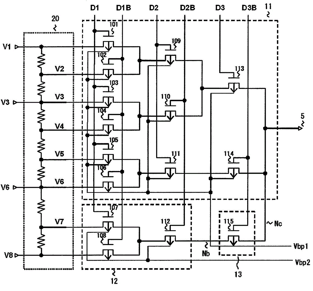
[0090] image 3 It is a figure which shows the structure of the 2nd Example of this invention. image 3 in, as figure 1 A specific example, expressing and figure 2 different compositions. refer to image 3 , this embodiment is to figure 2 The pMOS transistor 112 is included in the structure of the second sub-decoder 12, and the second back gate power supply Vbp2 is supplied to the back gate of the pMOS transistor 112. As the third sub-decoder 13, there is a pMOS transistor 115, one end (such as a source pole) receives the output of the second sub-decoder 12, the gate receives D3B, and the other end (for example, the drain) and the other end (for example, the drain) of the pMOS transistors 113 and 114 are commonly connected to the terminal 5, to the back of the pMOS transistor 115 The gate together with the back gate of the pMOS transistor of the first sub-decoder 11 provides the first back gate power supply Vbp1.

[0091] The first back gate power supply Vbp1 and fi...


PUM


Abstract

Disclosed is a decoder, receiving the first and the second reference voltage groups and selecting a reference voltage in accordance with a received digital signal, including a first sub-decoder receiving the first reference voltage group, a second sub-decoder receiving the second reference voltage group 20B, and a third sub-decoder receiving a reference voltage selected by the second sub-decoder and outputting the selected reference voltage to the first sub-decoder or an output terminal of the decoder. The first sub-decoder includes a transistor of a first conductivity type having a back gate supplied with a first power supply voltage, the second sub-decoder includes a transistor of the first conductivity type having a back gate supplied with a second power supply voltage, and the third sub-decoder includes a transistor of the first conductivity type having a back gate supplied with a first power supply voltage.

Description

technical field [0001] The present invention relates to a decoder which inputs a plurality of voltage signals and selectively outputs according to digital signals, and a data driver of a display device using the decoder. Background technique [0002] Figure 19 It is a diagram for explaining an example of a typical configuration of a decoding circuit of a data driver for a display element of a display panel by selecting one voltage (gradation voltage) from a plurality of reference voltages based on a video data signal. Also in Figure 19 For ease of description, the following structure is illustrated: the image data signal is a 3-bit digital signal (High indicates the high-order side power supply VDD, and Low indicates the low-order side power supply VSS), and the 3-bit data and its complementary signals D1, D1B, D2, D2B, D3, and D3B select and output one of the eight reference voltages V1-V8 in a competitive manner. That is, there are 14 pMOS transistors (transfer transist...

Claims


Application Information

Patent Timeline
Patent Type & Authority Patents(China)
IPC IPC(8): G09G3/20
CPCG09G3/3283G09G3/3291G09G3/3688G09G2310/027
Inventor 土弘土井延恭
Owner RENESAS ELECTRONICS CORP
Why Eureka
Try Eureka