

Step-type gan gate device and preparation method thereof
A stepped, gated technology, applied in semiconductor/solid-state device manufacturing, semiconductor devices, electrical components, etc., can solve the problem of inability to effectively improve the withstand voltage performance of GaN HEMT, reduce the gate size, improve the withstand voltage performance, The effect of easy process conditions
- Summary
- Abstract
- Description
- Claims
- Application Information
AI Technical Summary
Problems solved by technology
Method used
Image

Examples
Embodiment 1
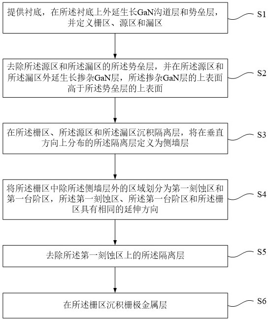
[0051] see Figure 1 to Figure 10 , this embodiment provides a method for preparing a stepped GaN gate device, which is characterized in that it includes the following steps:
[0052] 1) Provide a substrate, epitaxially grow a GaN channel layer and a barrier layer on the substrate, and define a gate region, a source region and a drain region;
[0053]2) removing the barrier layer of the source region and the drain region, and epitaxially growing a doped GaN layer on the source region and the drain region, the upper surface of the doped GaN layer being higher than the the upper surface of the barrier layer;
[0054] 3) Depositing an isolation layer on the gate region, the source region, and the drain region, and defining the isolation layer distributed in the vertical direction as a sidewall layer;
[0055] 4) Divide the area of the gate region except the sidewall layer into a zeroth etching region and a zeroth step region, the zeroth etching region, the zeroth step region ...
Embodiment 2
[0087] like Figure 10 As shown, this embodiment provides a stepped GaN gate device, which is characterized in that it includes:
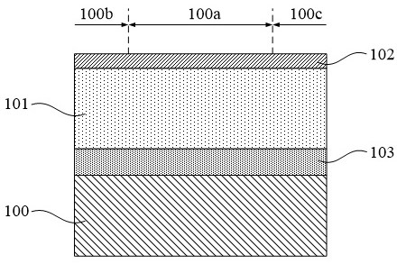
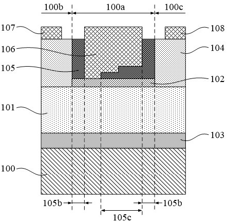
[0088] A substrate 100, on which a gate region 100a, a source region 100b and a drain region 100c are defined
[0089] A channel layer 101 and a barrier layer 102 are sequentially formed on the substrate 100, and the barrier layer 102 is located in the gate region 100a;
[0090] a doped GaN layer 104 formed in the source region 100b and the drain region 100c, the upper surface of which is higher than the upper surface of the barrier layer 102;
[0091] The sidewall isolation layer 105b formed on the sidewall of the doped GaN layer 104 and the step isolation layer 105c formed above the barrier layer 102; the region of the gate region 100a except the sidewall isolation layer 105b Divided into an etching region and a step region, the step region is adjacent to the doped GaN layer 104 on one side of the gate region 100a; the step isolation layer 105c...
PUM
| Property | Measurement | Unit |
|---|---|---|
| thickness | aaaaa | aaaaa |
Abstract
Description
Claims
Application Information