A method for preparing 10nm T-grid by electron beam exposure

A technology of electron beam exposure and electron beam lithography, which is applied in the manufacture of circuits, electrical components, semiconductors/solid-state devices, etc., can solve the problem of poor conformality of etched topography and poor resistance of photoresist to plasma etching , development process requirements are very high, etc., to achieve the effect of small etching size, reduced size, and high thickness

Inactive Publication Date: 2017-12-01
FUDAN UNIV
View PDF6 Cites 0 Cited by
  • Summary
  • Abstract
  • Description
  • Claims
  • Application Information

AI Technical Summary

Problems solved by technology

However, this method has the development interference of each layer, and has high requirements on the development process. It is necessary to strictly control the development time of each layer in order to obtain the T-shaped morphology;
[0008] 2. Affected by the proximity effect of electron beam lithography, when using a multi-layer adhesive structure, the bottom layer of photoresist PMMA or ZEP can only achieve a minimum of 30nm lines
[0009] Therefore, when the frequency of the device is to be further increased, the gate length of the device needs to be shorter, so a smaller-sized T-shaped gate is urgently needed. However, the minimum size of the multi-layer adhesive structure using electron beam lithography can only be achieved 30nm
Electron beam lithography combined with reactive ion etching process, the selectivity of etching can be used to prepare T-shaped gates with a size smaller than 30nm, the most important method is to use photoresist as a mask to etch silicon dioxide or silicon nitride Such a dielectric film, but using photoresist as a mask has its own defects. First, photoresist is not resistant to plasma etching, and the conformality of its etched morphology is not ideal. Secondly, photoresist and The etching selectivity ratio of the dielectric film will limit the thickness of the dielectric film. If the photoresist is too thick, the size of the foot will increase. If the photoresist is too thin, the dielectric film should be relatively thinner

Method used


Image

  • A method for preparing 10nm T-grid by electron beam exposure
  • A method for preparing 10nm T-grid by electron beam exposure
  • A method for preparing 10nm T-grid by electron beam exposure

Examples


Embodiment Construction

[0043] In order to make the object, technical solution and advantages of the present invention clearer, the present invention will be further described in detail below in conjunction with specific embodiments and with reference to the accompanying drawings.

[0044] The present invention is to fabricate a nanometer T-shaped gate structure on the device substrate as a gate, use electron beam lithography and reactive ion etching to form a T-shaped shape with a size of 10nm, and use thermal evaporation to evaporate the gate metal and peel off to obtain a T-shaped structure with a size of 10nm. The metal gate is compatible with the basic process for preparing HEMT devices, and can greatly reduce the size of the T-shaped gate.

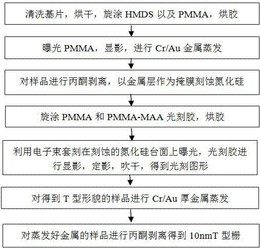
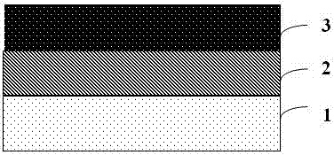
[0045] Figure 2-Figure 8 It is a flow chart of a method for preparing a 10nm T-shaped grid by electron beam lithography and reactive ion etching provided by the present invention, the method comprising:

[0046] Step 1: If figure 2 As shown, electron be...


PUM


Abstract

The present invention belongs to the technical field of micro-electronic components, and especially provides a method for manufacturing a 10-nanometer T-shaped gate through electron beam lithography. The method adopts the technology combining electron beam overlap lithography with reactive ion etching, and comprises the steps of applying electron beam photoresist to the surface of an epitaxial layer of a device substrate in a spin coating way, designing a layout through electron beam lithography, performing metal evaporation, stripping the evaporated metal, then performing reactive ion etching to form a table top, applying the electron beam photoresist to a sample with the etched table top in a spin coating way, utilizing the precise electron beam overlap lithography to form a T-shaped morphology, performing metal evaporation again, and stripping the evaporated metal to form a T-shaped metal electrode, thereby manufacturing a 10-nanometer T-shaped gate between a source electrode and a drain electrode of the device through the electron beam lithography. The method of the present invention not only can greatly reduce the foot size of the T-shaped gate, but also can manufacture the T-shaped gate having a very wide head, thereby reducing gate resistance of the device and raising cut-off frequency of the device, therefore, the method has important significance in a process for manufacturing GaN-based and InP-based high-electron-mobility transistors.

Description

technical field [0001] The invention belongs to the technical field of microelectronic components, and in particular relates to a method for preparing a 10-nanometer T-shaped grid by electron beam exposure. Background technique [0002] The HEMT high electron mobility transistor uses a heterojunction to realize a spatial separation of the electron supply layer and the electron transport channel layer, eliminating the scattering of electrons by the ionized donor impurities in the doped channel, so that the electron mobility in the channel is very high. High, so the transconductance of the device is large, the cut-off frequency is high, the noise is low, the switching speed is fast, and it can be successfully applied in the field of microwave low-noise amplification. The high-frequency performance of the HEMT device is directly related to the processing technology of the device, especially the fabrication of the grid lines plays a decisive role in the cut-off frequency of the ...

Claims


Application Information

Patent Timeline
Patent Type & Authority Patents(China)
IPC IPC(8): H01L21/28
CPCH01L21/28079
Inventor 陈宜方邵金海陆冰睿
Owner FUDAN UNIV
Why Eureka
Try Eureka