Image display device and manufacturing method thereof

a technology of image display and manufacturing method, which is applied in the direction of semiconductor/solid-state device manufacturing, semiconductor devices, electrical apparatus, etc., can solve the problems of reducing the aperture ratio of a pixel, affecting the processing accuracy and affecting the size of thin film transistors or the like within the pixel, so as to improve the aperture ratio and reduce the size of the gate electrode. , the effect of improving the aperture ratio

Active Publication Date: 2013-05-07
PANASONIC INTELLECTUAL PROPERTY CORP OF AMERICA +1
View PDF8 Cites 0 Cited by
  • Summary
  • Abstract
  • Description
  • Claims
  • Application Information

AI Technical Summary

Benefits of technology

[0010]The present invention has been made in view of the above-mentioned problems, and therefore has an object to provide an image display device capable of reducing a photoleakage current of a thin film transistor and also improving an aperture ratio of a pixel.
[0013]According to the present invention, the size of the gate electrode may be reduced while avoiding the semiconductor layer from extending off the gate electrode, and hence the photoleakage current of the thin film transistor may be reduced and also the aperture ratio of the pixel can be improved. Further, with the suppression of the photoleakage current and the improvement of the aperture ratio, a high contrast liquid crystal display device may be manufactured in low cost.

Problems solved by technology

However, in the conventional liquid crystal display device, it is known that, even when the thin film transistor is OFF, electric charges leak from the storage capacitor due to a backlight beam from the backlight unit.
In this case, there is a fear of reduction in aperture ratio of a pixel.
Meanwhile, the size of the thin film transistor or the like within the pixel is limited by the processing accuracy and the drive ability thereof, and hence there is a demand for a thin film transistor having a smaller occupied area.

Method used


Image

  • Image display device and manufacturing method thereof
  • Image display device and manufacturing method thereof
  • Image display device and manufacturing method thereof

Examples


first embodiment

[First Embodiment]

[Overall Structure]

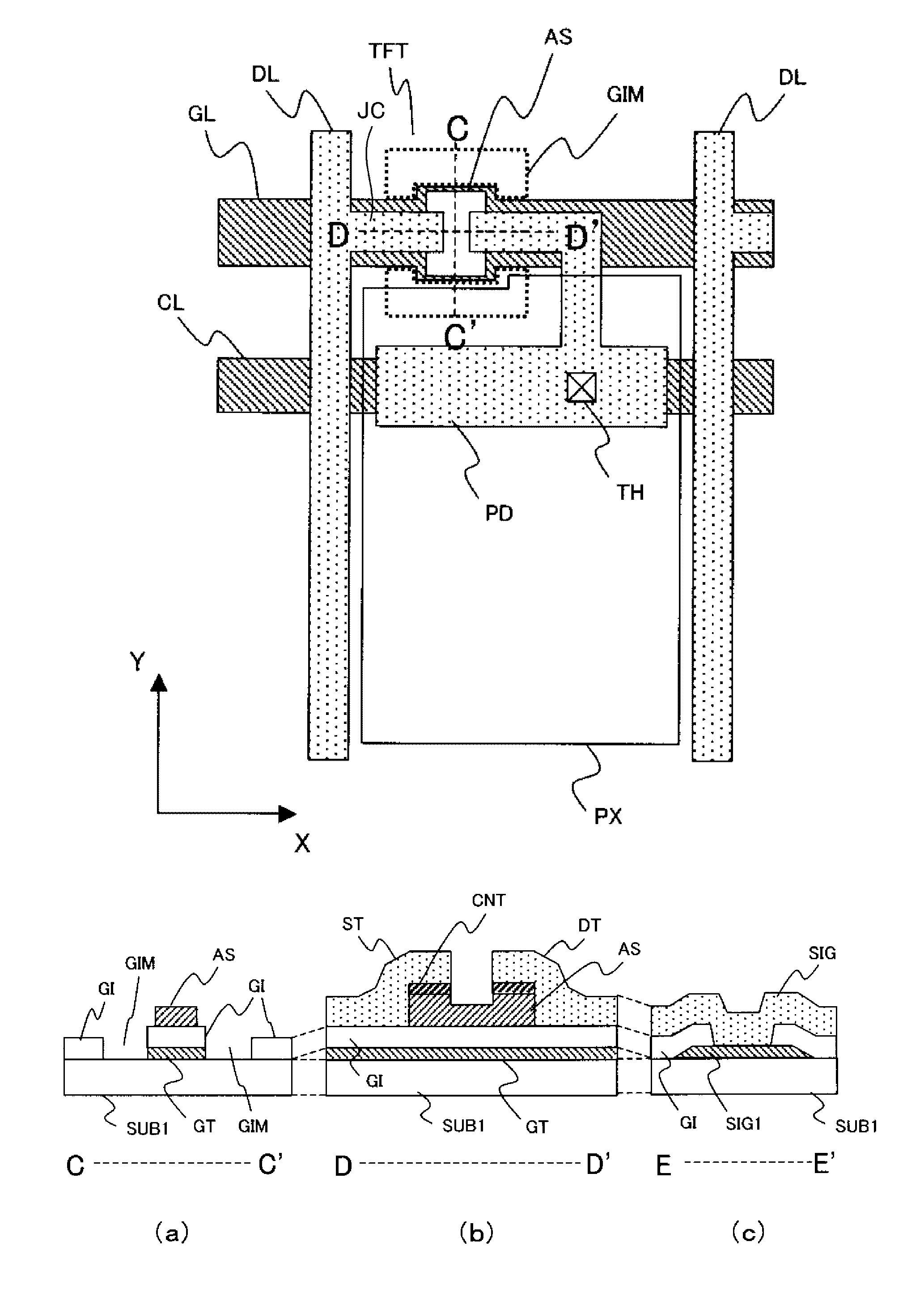
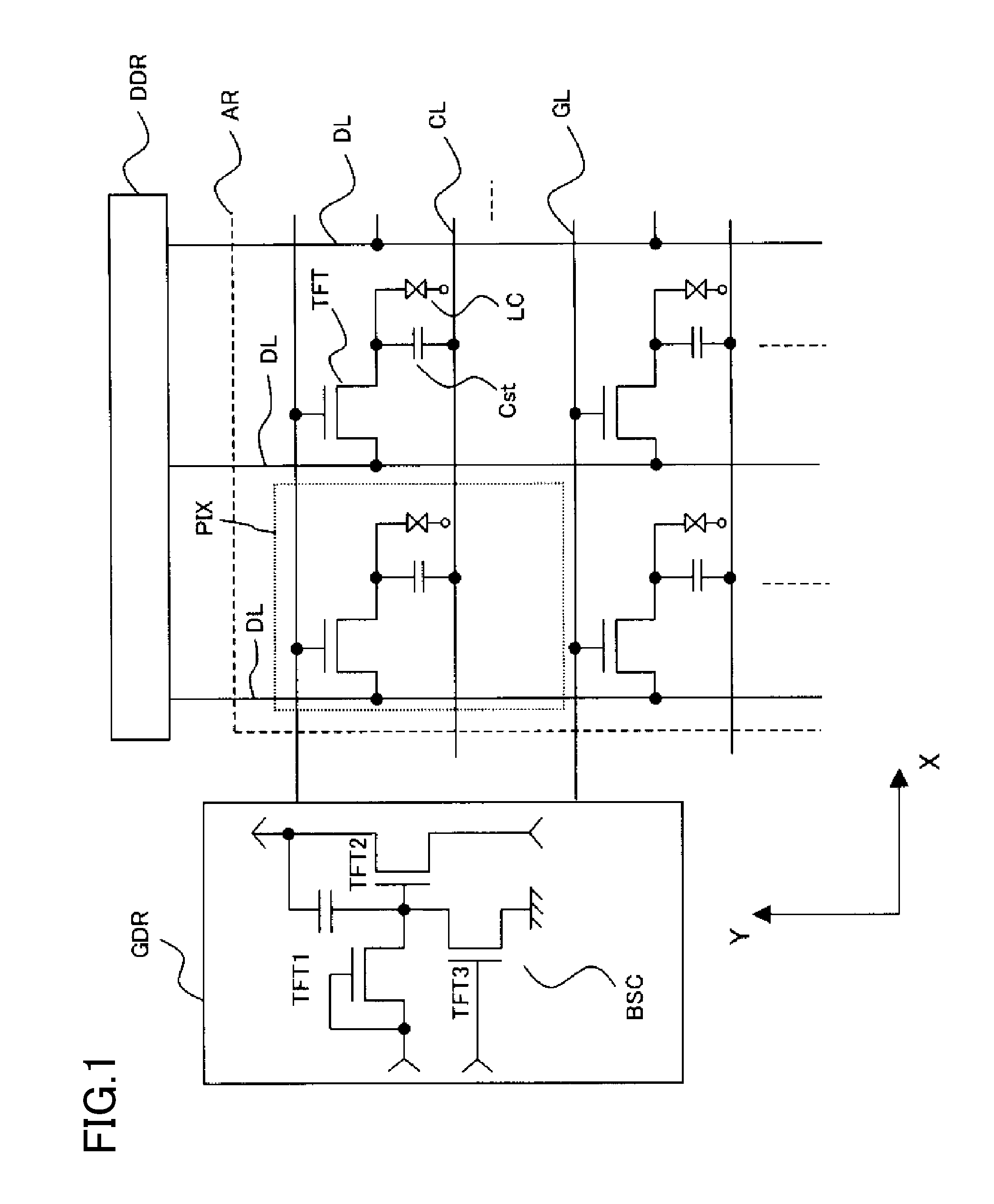
[0046]FIG. 1 is a diagram illustrating a schematic structure of a liquid crystal display device, which is an example of an image display device according to a first embodiment of the present invention. Hereinafter, with reference to FIG. 1, an overall structure of the liquid crystal display device of the first embodiment is described. Note that, symbols X and Y illustrated in FIG. 1 represent an X-axis and a Y-axis, respectively. Further, in the following description, a video signal line formed within a display region, for supplying a video signal (drain signal) to each pixel is represented as a drain line, and a scan signal line for supplying a scan signal (gate signal) which controls ON / OFF of a thin film transistor in each pixel is represented as a gate line. Further, the following description is given assuming the case where the present invention is applied to a TN type liquid crystal display device, but the present invention is also applicab...

second embodiment

[Second Embodiment]

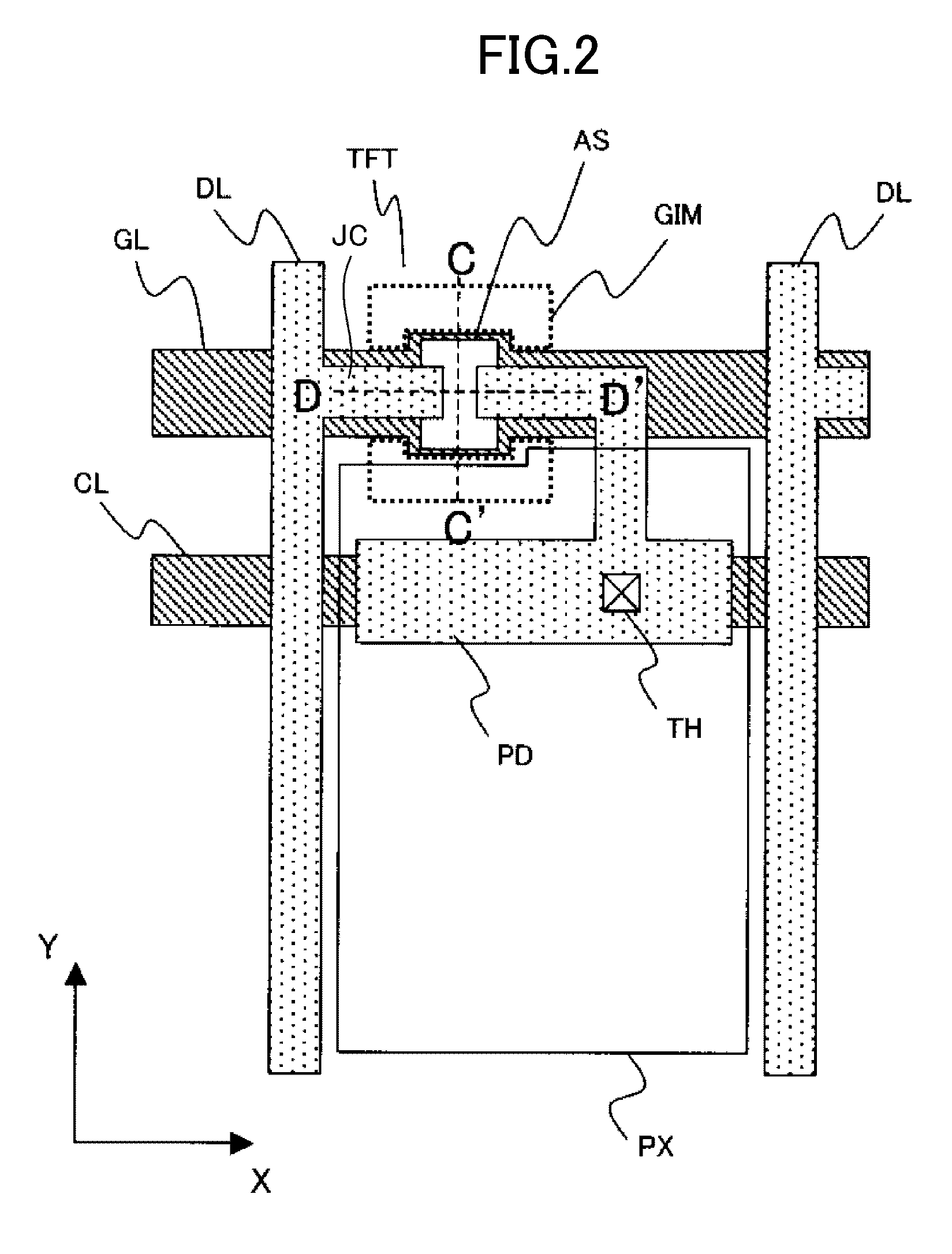
[0078]FIG. 9 is a plan view illustrating a pixel structure of an image display device according to a second embodiment of the present invention. FIG. 10 is a plan view illustrating a schematic structure of a bootstrap circuit forming a peripheral circuit of the image display device according to the second embodiment of the present invention. Hereinafter, with reference to FIGS. 9 and 10, a pixel and the peripheral circuit of the liquid crystal display device, which is the image display device of the second embodiment, are described. Note that, the liquid crystal display device of the second embodiment is different from that of the first embodiment only in the structure of the thin film transistor TFT, and other structures of the second embodiment are the same as those of the first embodiment. Therefore, in the following description, the structure of the thin film transistor TFT is described in detail. Further, the thin film transistor TFT of the second embodiment ...

third embodiment

[Third Embodiment]

[0116]FIG. 22 is a cross-sectional view of a liquid crystal display device according to a third embodiment of the present invention, and particularly illustrates a TN type liquid crystal display device using the first substrate on which the thin film transistors of the first embodiment are formed. However, the present invention is not limited to the TN type liquid crystal display device, and is also applicable to a VA type liquid crystal display device, in which the pixel electrode and the common electrode are formed on different substrates similarly to the TN type liquid crystal display device, or an IPS type liquid crystal display device. Note that, structures other than the structure of the thin film transistor TFT formed within the display region of the first substrate SUB1 are the same as those of the conventional liquid crystal display device.

[0117]As illustrated in FIG. 22, the liquid crystal display device of the third embodiment includes a glass substrate ...


PUM


Abstract

Provided is an image display device including thin film transistors on a substrate, including: gate lines and drain lines intersecting the gate lines, each thin film transistor having, in a channel region, a laminate structure in which a gate electrode, a gate insulating film, and a semiconductor layer are laminated in the stated order from the substrate side; and a pair of removal regions in which parts of the gate insulating film are removed, which are formed on both sides of the gate electrode and formed in a channel width direction of the channel region, in which when W represents a width of the gate electrode in the channel width direction of the channel region, and R represents a width of the gate insulating film in the channel width direction, which is sandwiched between the pair of removal regions, R≧W is satisfied.

Description

CROSS-REFERENCE TO RELATED APPLICATION[0001]The present application claims priority from Japanese application JP 2010-098486 filed on Apr. 22, 2010, the content of which is hereby incorporated by reference into this application.BACKGROUND OF THE INVENTION[0002]1. Field of the Invention[0003]The present invention relates to an image display device and a manufacturing method therefor. In particular, the present invention relates to an image display device in which an aperture ratio of a pixel may be improved and a manufacturing method therefor.[0004]2. Description of the Related Art[0005]A conventional liquid crystal display device includes a non-emissive type liquid crystal display panel and a backlight unit, which illuminates the liquid crystal display panel from a rear surface side thereof. In the liquid crystal display panel, thin film transistors are formed in respective pixels. In each of the pixels, which are formed in matrix in a display region, there are provided a storage ca...

Claims


Application Information

Patent Timeline
Patent Type & Authority Patents(United States)
IPC IPC(8): H01L29/04H01L29/10H01L31/036H01L21/84
CPCH01L29/42384H01L29/66765H01L27/1248H01L29/78696H01L29/78621
Inventor TOYOTA, YOSHIAKI
Owner PANASONIC INTELLECTUAL PROPERTY CORP OF AMERICA
Why Eureka
Try Eureka