Magnetic tunnel junction memory device

a magnetic tunnel junction and memory device technology, applied in the direction of information storage, static storage, digital storage, etc., can solve the problems of limiting the density of mtj cells in a mram array, affecting the stability of mtj elements with sub-micron dimensions at elevated temperature of operation, and affecting the stability of mtj elements with sub-micron dimensions, etc., to achieve addressing errors, high density, and improve spin-dependent tunneling

Inactive Publication Date: 2005-01-18
SHUKH ALLA MIKHAILOVNA
View PDF17 Cites 198 Cited by
  • Summary
  • Abstract
  • Description
  • Claims
  • Application Information

AI Technical Summary

Benefits of technology

The magnetic flux guide consists at least of a bottom magnetic portion and a top magnetic portion with the MTJ element positioned between the portions. The magnetic flux guide provides an effective magnetic flux supply to the MTJ element for reducing a write current in a “write” mode or an excitation current in a “read” mode of operation. The magnetic flux guide is made of a conductive magnetic material having a high magnetic permeability and a low electrical resistivity. The pinned and free layers of the MTJ element are magnetically isolated from the magnetic flux guide by thin non-magnetic conductive spacers. This prevents undesirable effects of the magnetic flux guide on a magnetic state of the pinned and free layers.
The MTJ memory cell according to the present invention can have several embodiments, which are not limited to the following:to enhance spin-dependent tunneling, the MTJ element can employ at least one spin polarizing layer, which can be positioned on one or both sides of the tunnel barrier layer between the tunnel barrier layer and one or both magnetic layers;to stabilize domain structure of the pinned layer for reducing addressing errors, the MTJ element can employ an antiferromagnetic layer having direct contact with the pinned layer and providing an antiferromagetic exchange coupling with the pinned layer;to increase memory cell density in the MRAM array, at least one of the read conductive lines can have a multilayer structure being composed at least of one magnetic conductive layer and one non-magnetic conductive layer having the magnetic conductive layer being positioned adjacent the MTJ element or the magnetic flux guide.
Switching field of TMJ memory element with perpendicular orientation of magnetization in the free and pinned layers has a marginal dependence on a junction size. This results from a weak dependence of the demagnetizing field in the pinned and free layers with a perpendicular anisotropy on the junction size. Therefore, the MRAM arrays with MTJ cells according to the present invention can have high density; high magnetic stability, low error rate and high reliability. Positioning of the MTJ memory element between portions of the magnetic flux guide allows substantial reduction of the write current.

Problems solved by technology

This limits the density of MTJ cells in a MRAM array.(b) The specified elongated shape of the MTJ elements is difficult to reproduce in sub-micron range of dimensions across a MRAM array composed of thousand elements.
Therefore, accidental reverse of the adjacent elements simply by the effect of the magnetic field produced along one of the addressing lines, bit or word, increases.(c) Number of addressing error in a MRAM array with in-plane orientation of magnetization increases with cell density increase.(d) The MTJ elements with sub-micron dimensions suffer from instability at elevated temperature of operation.
All above-mentioned disadvantages limit an application of the MTJ memory cells with in-plane orientation of magnetization in the magnetic layers for high-density MRAM arrays.

Method used


Image

  • Magnetic tunnel junction memory device
  • Magnetic tunnel junction memory device
  • Magnetic tunnel junction memory device

Examples


Embodiment Construction

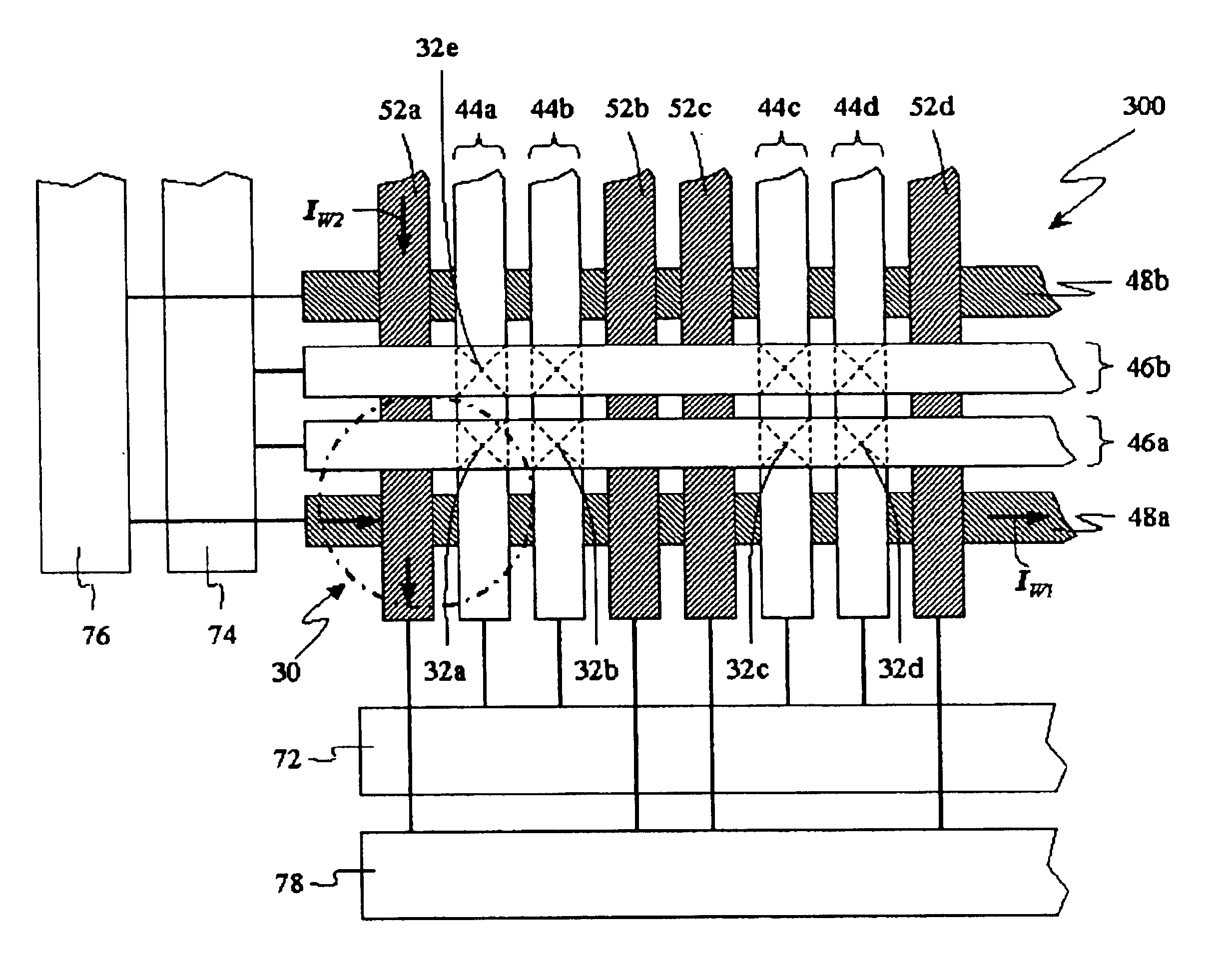
A MTJ memory cell of the present invention utilizes a phenomenon of a tunneling giant magnetoresistance in sandwiched magnetic and insulating layers. The memory cell employs a MTJ memory element formed by two magnetic layers with perpendicular anisotropy having different coercive forces, which are separated by a thin insulating layer as a tunneling barrier.

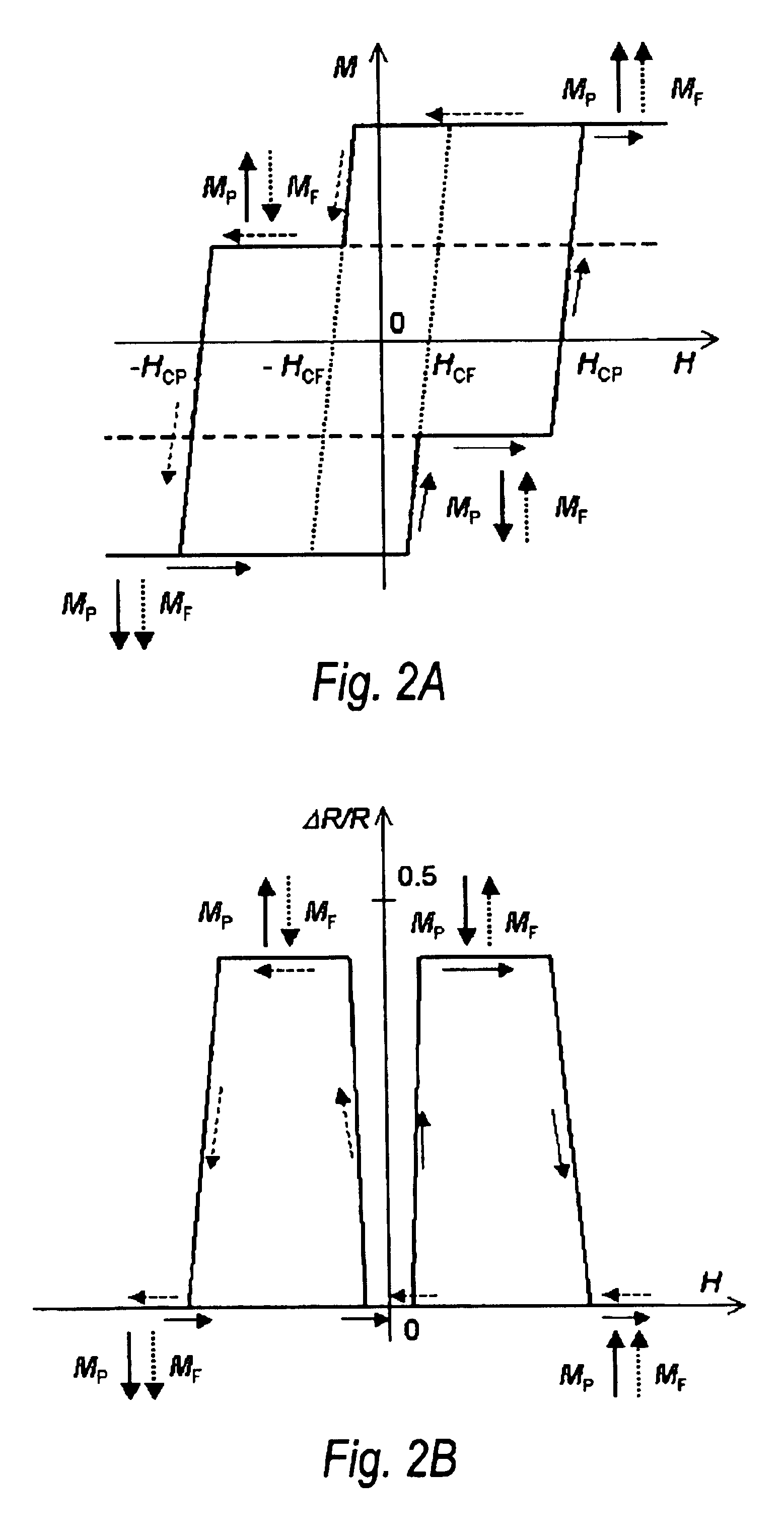
FIGS. 2A and 2B illustrate a MH-loop and a MR-curve of the MTJ element with the perpendicular anisotropy in the free and pinned magnetic layers when an external magnetic is applied perpendicular to a major plane of the layers. HCF and HCP is a coercivity of the free and pinned layers, respectively. Arrows denote orientation of the magnetization in the pinned and free layers. The dot arrow corresponds to the magnetization orientation in the free layer. The dash arrow represents the orientation of the magnetization in the pinned layer. A dot line in the FIG. 2A represents a MH-loop of the free layer. A dash line gives the MH-loop of...


PUM


Abstract

A memory cell for magnetic random access memory devices based on a magnetic tunnel junction (MTJ) memory element with a perpendicular orientation of magnetization in pinned and free magnetic layers, and a tunnel barrier layer sandwiched between the pinned and free layers. The memory cell can include the MTJ memory element, a magnetic flux guide in series with selection devices, such as a bit line, a word line, and a transistor. The magnetic flux guide can have two electrically conductive magnetic portions with the MTJ memory element positioned between the magnetic portions. The MTJ memory element is magnetically isolated from the magnetic flux guide by thin non-magnetic conductive spacers. The MTJ memory element is arranged in a vertical space between the intersecting bit and word lines at their intersection region. The memory cell also includes write and excitation lines. The write line is parallel to the bit line and the excitation line is parallel to the word line. The write and excitation lines also intersect each other and define a corner. The MTJ memory element is positioned in the corner of the intercepting write and excitation lines.

Description

FIELD OF THE INVENTIONThe present invention relates generally to the field of non-volatile memory devices for use in computers and other devices. More particularly, the present invention relates to a magnetic tunnel junction memory cell with a perpendicular orientation of magnetization in free and pinned layers of a magnetic tunneling junction memory element that is used as an individual memory cell of non-volatile magnetic random access memory arrays.BACKGROUND OF THE INVENTIONThe use of a magnetic tunnel junction element in a memory cell of a non-volatile magnetic random access memory (MRAM) arrays is described in U.S. Pat. No. 5,640,343. A typical MRAM device includes an array of memory cells positioned at the intersections of word lines and bit lines.A typical memory cell may be composed of a magnetic tunnel junction (MTJ) memory element and a transistor or other non-linear element in series, and intersecting conductive lines. The memory cell is controlled by passing currents th...

Claims


Application Information

Patent Timeline
Patent Type & Authority Patents(United States)
IPC IPC(8): G11C11/14G11C11/02
CPCG11C11/14
Inventor SHUKH, ALLA MIKHAILOVNA
Owner SHUKH ALLA MIKHAILOVNA
Why Eureka
Try Eureka