Phase changeable memory device and method of formation thereof

a memory device and phase change technology, applied in the direction of semiconductor devices, basic electric elements, electrical equipment, etc., can solve the problems of large current required at the time of programming, loss of heat, and large amount of current required to supplement the loss of heat, so as to achieve the effect of reducing the current of the program

Active Publication Date: 2006-05-25
SAMSUNG ELECTRONICS CO LTD
View PDF9 Cites 189 Cited by
  • Summary
  • Abstract
  • Description
  • Claims
  • Application Information

AI Technical Summary

Benefits of technology

[0007] It is an object of the present invention to provide a phase changeable memory device in which the occurrence of a distribution failure of a resistor is mitigated or eliminated, and in which program current is effectively reduced, and a method of formation thereof.

Problems solved by technology

However, in a conventional structure where the lower electrode contact directly contacts the phase changeable layer, a large amount of current is required at the time of programming.
Since thermal conductivity of the phase changeable layer is high, any heat that is present at the interface between the lower electrode contact and the phase changeable layer is output through the phase changeable layer, thereby causing a loss of heat.
However, a great deal of current is required for supplementing the lost heat.
However, in the above structure of forming a memory device, the etching gas can react with a lower electrode layer to form an undesirable oxide layer and a fluoric layer at the interface,. thereby causing a resistor distribution failure.

Method used


Image

  • Phase changeable memory device and method of formation thereof
  • Phase changeable memory device and method of formation thereof
  • Phase changeable memory device and method of formation thereof

Examples


Embodiment Construction

[0031] The present invention will now be described more fully hereinafter with reference to the accompanying drawings, in which preferred embodiments of the invention are shown. This invention may, however, be embodied in different forms and should not be constructed as limited to the embodiments set forth herein. Rather, these embodiments are provided so that this disclosure will be thorough and complete, and will fully convey the scope of the invention to those skilled in the art. In the drawings, the thickness of layers and regions are exaggerated for clarity. It will also be understood that when a layer is referred to as being “on” another layer or substrate, it can be directly on the other layer or substrate or intervening layers may also be present. Like numbers refer to like elements throughout the specification.

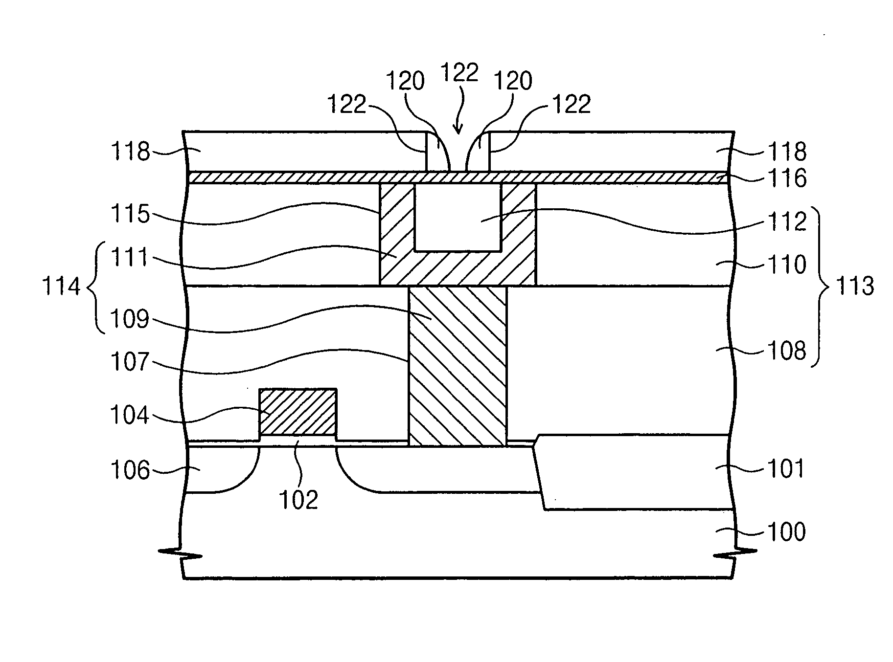
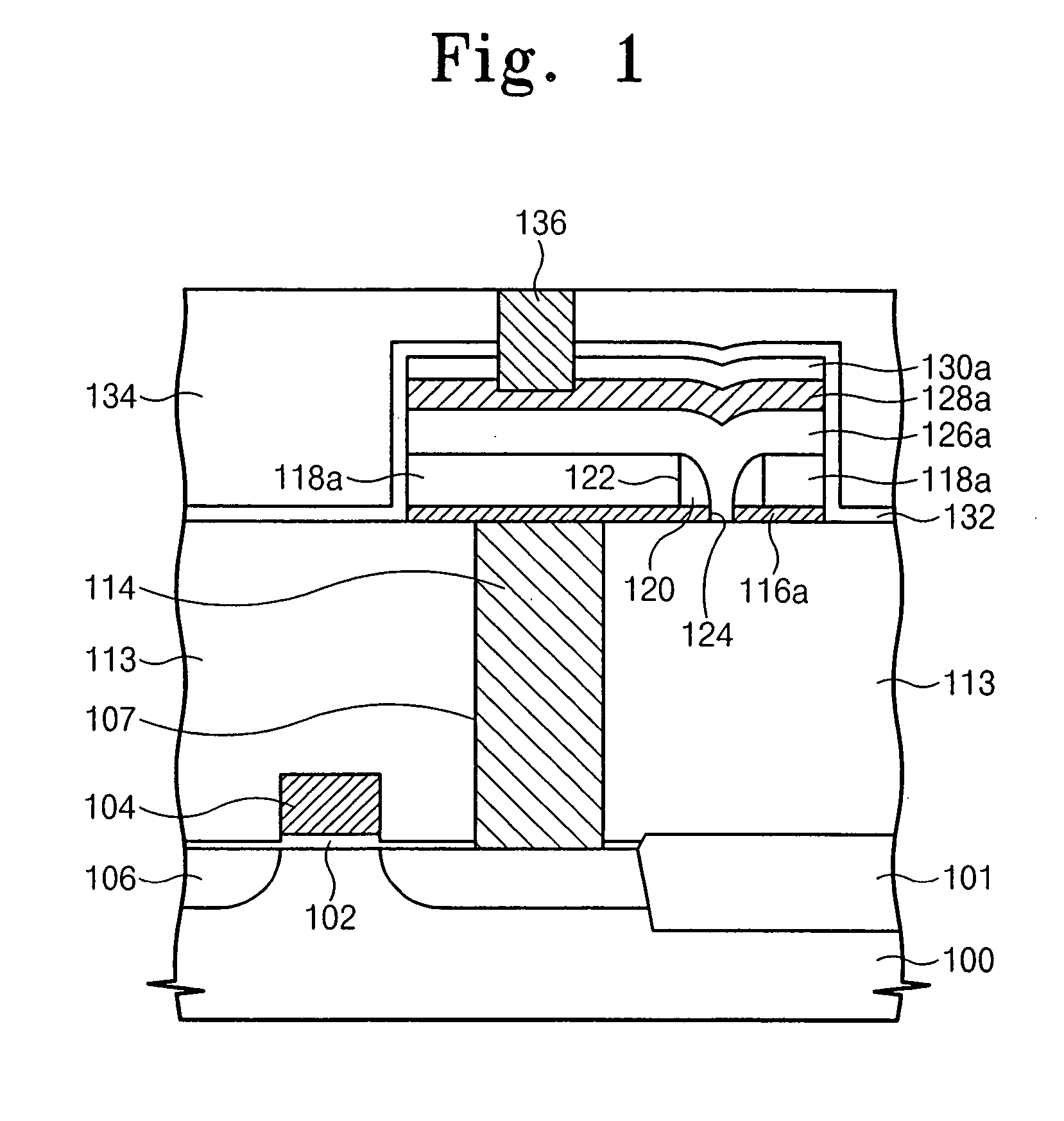
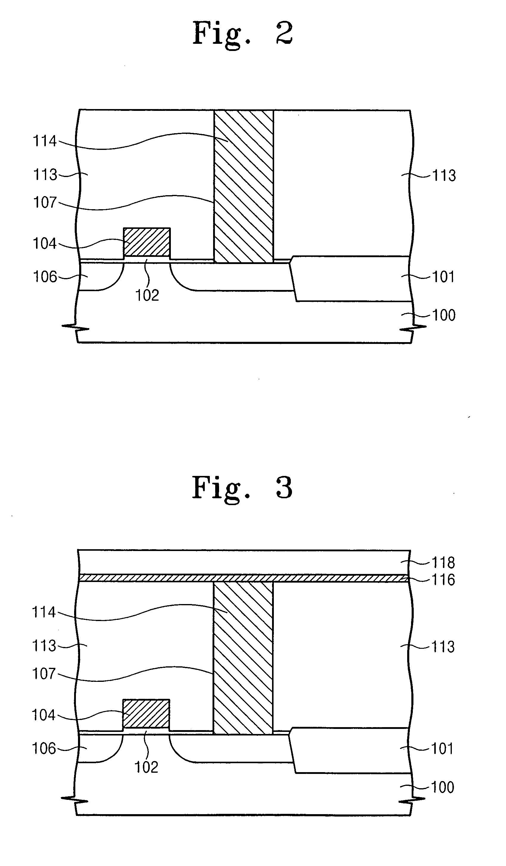
[0032]FIG. 1 is a cross-sectional view of a phase changeable memory device in accordance with an embodiment of the present invention.

[0033] Referring to FIG. 1, a g...


PUM


Abstract

In a phase changeable memory device and a method of formation thereof, the phase changeable memory device comprises: a lower electrode pattern on an interlayer insulating layer; an insulating pattern located on the lower electrode pattern; a phase changeable pattern penetrating the insulating pattern and the lower electrode pattern to contact the lower electrode pattern and the interlayer insulating layer; and an upper electrode on the phase changeable pattern.

Description

CROSS-REFERENCE TO RELATED APPLICATIONS [0001] This U.S. non-provisional patent application claims priority under 35 U.S.C. § 119 of Korean Patent Application 10-2004-0083690 filed on Oct. 19, 2004, the entire contents of which are incorporated herein by reference. BACKGROUND OF THE INVENTION [0002] The present invention relates to a non-volatile memory device and a method thereof, and more particularly, to a phase changeable memory device and a method of formation thereof. [0003] Non-volatile memory devices share a common characteristic in that they retain stored data even though the power supply is interrupted. Contemporary non-volatile memory devices commonly employ flash memory cells having a stacked gate structure. The stacked gate structure includes a tunnel oxide layer, a floating gate, a gate interlayer dielectric layer and a control gate electrode, which are sequentially stacked. In order to improve reliability of the flash memory cells and programming efficiency, the chara...

Claims


Application Information

Patent Timeline
Patent Type & Authority Applications(United States)
IPC IPC(8): H01L21/20H01L21/8244
CPCH01L45/06H01L45/1233H01L45/126H01L45/144H01L45/1666H01L27/2436H01L45/122H10B63/30H10N70/821H10N70/8413H10N70/231H10N70/061H10N70/8828H10N70/826
Inventor CHO, BYEONG-OKJOO, SUK-HORYOO, KYUNG-CHANGBYUN, KYUNG-RAE
Owner SAMSUNG ELECTRONICS CO LTD
Why Eureka
Try Eureka