Vacuum imprinting device, vacuum compressing device and manufacturing method of layered optical component

A manufacturing method, vacuum lamination technology, applied to lamination devices, optical components, chemical instruments and methods, etc., can solve problems such as process instability, insufficient lamination precision, easy introduction of air bubbles during lamination and rolling, etc. Achieve the effect of improving process precision, suppressing bubble phenomenon, and eliminating instability

Inactive Publication Date: 2011-09-07
AU OPTRONICS CORP
View PDF8 Cites 20 Cited by
  • Summary
  • Abstract
  • Description
  • Claims
  • Application Information

AI Technical Summary

Problems solved by technology

In the rolling process, the operator needs to align the template or protective film with the optical adhesive layer, and then use the rolling wheel to roll, which will easily lead to insufficient lamination accuracy, and easy to introduce air bubbles during lamination and rolling , Rolling is not easy to control the lamination gap and the machine needs to be moved before curing, which may cause variation in the thickness of the optical adhesive layer
In addition, in the process of forming the optical layer using the rolling process using a template, the template still needs to be manually demoulded after the optical adhesive layer is cured. However, due to the large uncertainties in the manual demoulding operation, it is easy to produce problem of instability

Method used


Image

  • Vacuum imprinting device, vacuum compressing device and manufacturing method of layered optical component
  • Vacuum imprinting device, vacuum compressing device and manufacturing method of layered optical component
  • Vacuum imprinting device, vacuum compressing device and manufacturing method of layered optical component

Examples


Embodiment Construction

[0040] Below in conjunction with accompanying drawing, structural principle and working principle of the present invention are specifically described:

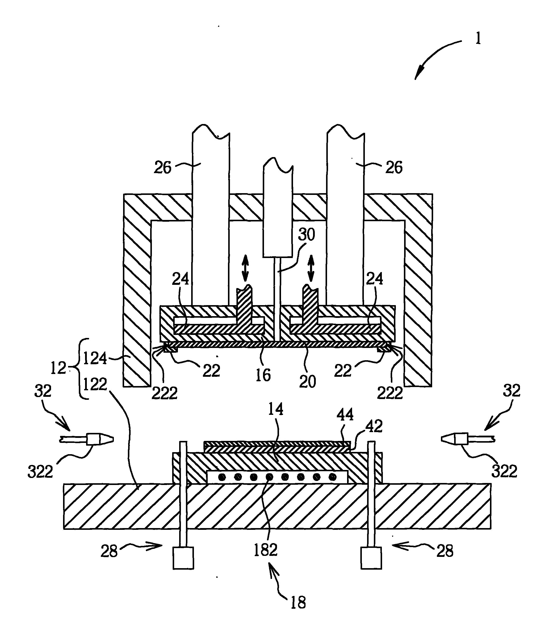
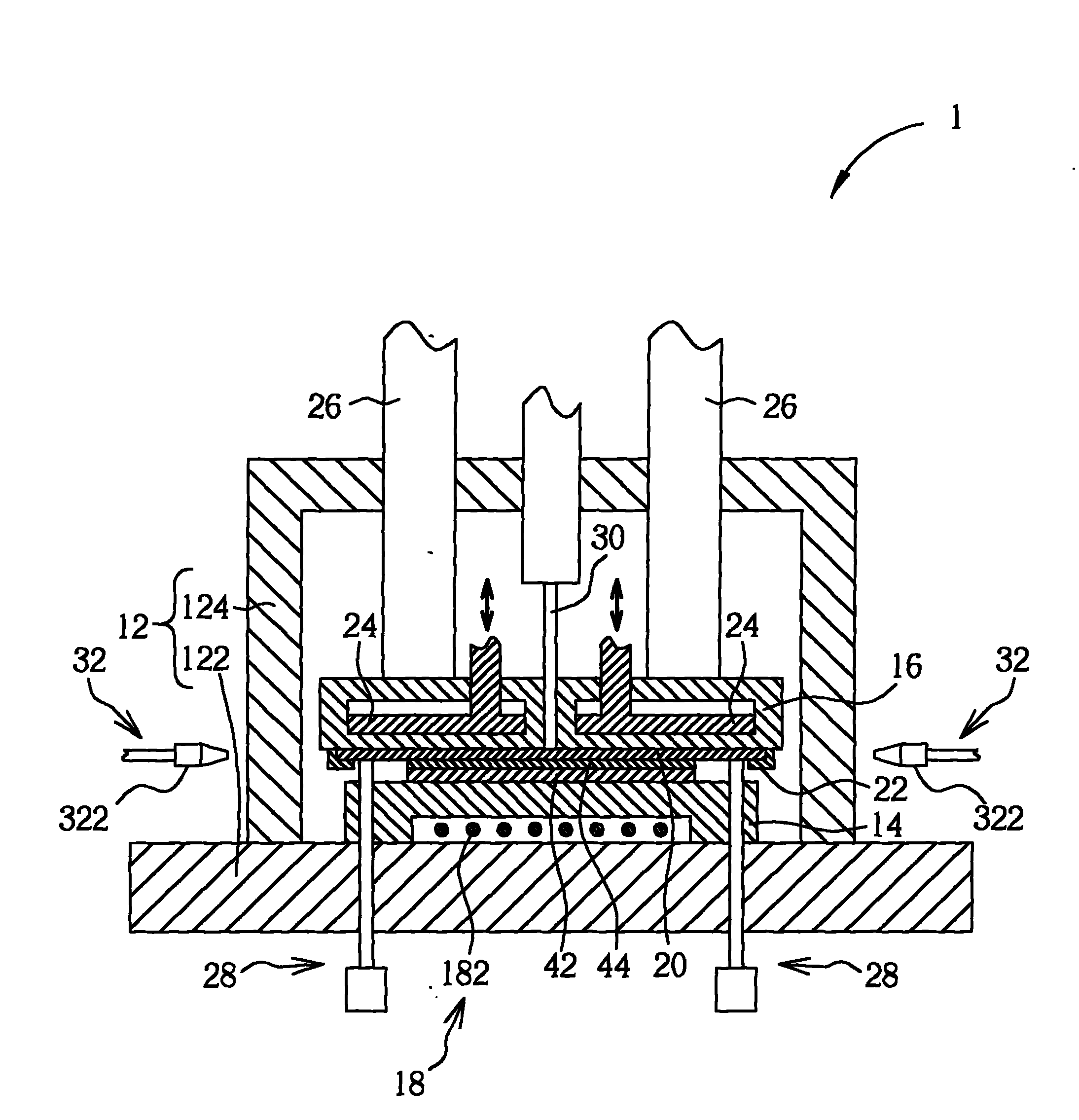
[0041] see figure 1 and figure 2 , figure 1 It is a schematic diagram of a vacuum imprinting device 1 according to a preferred embodiment of the present invention, figure 2 for figure 1 A schematic diagram of the medium-vacuum imprinting device 1 in another state. The vacuum imprinting device 1 includes a vacuum chamber 12 , a loading platform 14 , an loading platform 16 and a curing device 18 . The vacuum chamber 12 is mainly composed of a base plate 122 and a cover body 124, the cover body 124 can be separated from the base plate 122 for the operation of inserting the object; when the base plate 122 and the cover body 124 are closed, as figure 2 As shown, the vacuum chamber 12 can be evacuated, and the evacuation device is a prior art, not otherwise described and shown in the figure. The loading platform 14 is dispo...


PUM


Abstract

The invention discloses a vacuum imprinting device, a vacuum compressing device and a manufacturing method of a layered optical component, wherein, the vacuum imprinting device and the vacuum compressing device respectively comprise a vacuum chamber, a downloading platform, an uploading platform and a curing device. The uploading platform which is opposed to the downloading platform is equipped inside the vacuum chamber and moving towards the downloading platform so as to apply imprinting or flatting operations. The curing device is used for curing an optical glue layer in order to form an optical layer. The manufacturing method comprises the steps of respectively applying the vacuum imprinting device and the vacuum compressing device on a base plate to form a plurality of optical layers and then shaping layered optical components. By applying devices in vacuum conditions so as to form optical glue layers, a bubble phenomenon generated in the layered structure of the optical layers after the optical layers are cured is effectively prevented in the invention.

Description

technical field [0001] The invention relates to a method for manufacturing a layered optical component and an embossing device and a laminating device thereof, in particular to a method for manufacturing a layered optical component using a vacuum process and a vacuum embossing device and a vacuum laminating device for it. Background technique [0002] The prior art layered optical components are manufactured by forming multi-layer optical layers on a substrate, and the multi-layer optical layers are sequentially cured by optical glue, wherein patterns can be printed on the optical layer by using a template as required. In the process of the prior art, the layered optical component is sequentially fabricated and formed in an atmospheric environment through processes such as coating, rolling, and curing. In the rolling process, the operator needs to align the template or protective film with the optical adhesive layer, and then use the rolling wheel to roll, which will easily ...

Claims


Application Information

Patent Timeline
Patent Type & Authority Applications(China)
IPC IPC(8): B41K3/02B32B37/10G02B1/12
Inventor 刘荣井黄建森赵文魁
Owner AU OPTRONICS CORP
Why Eureka
Try Eureka