Touch control panel structure and manufacture method thereof

A technology for a touch panel and a manufacturing method, which are applied in the fields of instruments, electrical digital data processing, and data processing input/output processes, etc., can solve the problems of consuming a lot of production materials, increasing the thickness of steps, and defective products.

Inactive Publication Date: 2011-10-05
WINTEK CORP +1
View PDF3 Cites 17 Cited by
  • Summary
  • Abstract
  • Description
  • Claims
  • Application Information

AI Technical Summary

Problems solved by technology

[0002] The existing touch panel structure, whether it is a single-plate touch panel or a double-plate touch panel, is formed on a transparent conductive substrate by performing a multi-channel screen printing process or a yellow photoetching process. The material of the transparent conductive substrate is mostly glass or plastic. Due to the high unit price of the transparent conductive substrate, a lot of production materials will be repeatedly consumed during manufacture. Wasteful, and the transparent conductive substrate is not easy to be made into a curved touch panel, and it is easy to cause defective products
[0003] In addition, the touch panel must be attached to a protective lens to be assembled into a finished product.

Method used


Image

  • Touch control panel structure and manufacture method thereof
  • Touch control panel structure and manufacture method thereof
  • Touch control panel structure and manufacture method thereof

Examples


Embodiment Construction

[0044] The technical means and effects used by the present invention to achieve the purpose will be described below with reference to the accompanying drawings, and the embodiments listed in the following drawings are only auxiliary explanations to facilitate the understanding of the review committee, but the technical means of this case are not Not limited to the figures listed.

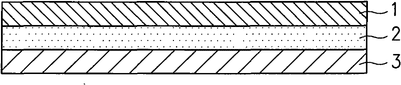
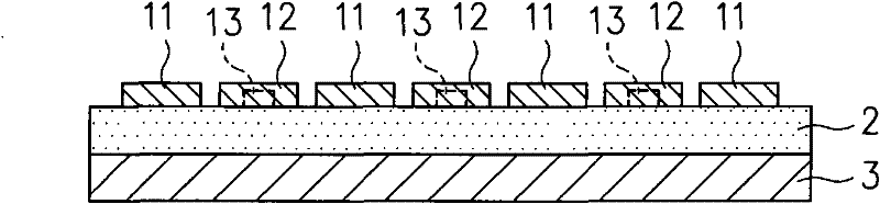
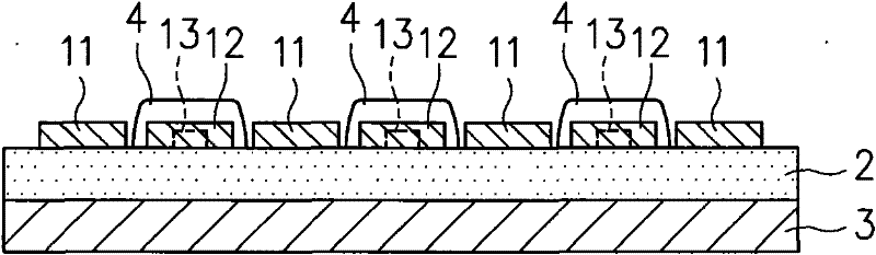
[0045] see Figure 1 to Figure 7 A schematic flow chart showing the forming process of the first embodiment of the touch panel structure of the present invention is shown.

[0046] First, if figure 1 As shown, a transparent conductive film 1 is prepared. One side of the transparent conductive film 1 is provided with an adhesive layer 2. The adhesive layer 2 is a transparent photosensitive adhesive. The transparent conductive film 1 is not provided on the adhesive layer 2. A release film 3 is provided on one side of the transparent conductive film 1, and then patterning processes such as wet etchin...


PUM


Abstract

The invention provides a touch control panel structure and a manufacture method thereof. In the invention, a conductive structure layer is formed on at least one adhesive layer; the conductive structure layer comprises at least one first conductor and at least one second conductor; and an insulation layer is arranged between the first conductor and the second conductor so that the first conductoris insulated from the second conductor. The purposes of saving production materials, reducing cost, improving product good rate, simplifying panel laminating procedure, attaching the touch control panel to object surfaces of arbitrary curved surfaces or plane surfaces, and facilitating design of thinned products and the like are achieved.

Description

technical field [0001] The present invention relates to a touch panel structure and manufacturing method, especially to a touch panel formed on an adhesive layer, which not only saves production materials, reduces costs, improves product yield, and simplifies the panel lamination process, The structure and manufacturing method of the touch panel can be attached to any curved or flat object surface, and at the same time, it is beneficial to the thin design of the product. Background technique [0002] The existing touch panel structure, whether it is a single-plate touch panel or a double-plate touch panel, is formed on a transparent conductive substrate by performing a multi-channel screen printing process or a yellow photoetching process. The material of the transparent conductive substrate is mostly glass or plastic. Due to the high unit price of the transparent conductive substrate, a lot of production materials will be repeatedly consumed during manufacture. It is waste...

Claims


Application Information

Patent Timeline
IPC IPC(8): G06F3/041
CPCG06F2203/04103
Inventor 林怡君吴明坤李晓萍黄炳文
Owner WINTEK CORP
Why Eureka
Try Eureka