Method for doping fin field-effect transistors

A fin-type field effect and transistor technology, which is applied in semiconductor devices, semiconductor/solid-state device manufacturing, electrical components, etc., to achieve the effect of improving electrical properties

Inactive Publication Date: 2011-11-09
TAIWAN SEMICON MFG CO LTD
View PDF6 Cites 34 Cited by
  • Summary
  • Abstract
  • Description
  • Claims
  • Application Information

AI Technical Summary

Benefits of technology

The technical effect that this patented method improves upon existing methods by providing better control over how well different layers are formed during manufacturing. This helps prevent problems such as unwanted deposition or contamination on other parts of the chip caused by insufficient heat treatment at certain points within each step.

Problems solved by technology

This patented technical problem addressed in the patents relates to improving the performance of CMOS FINFET devices during rapid progressive scaling while reducing issues with dopants being introduced due to tilting or misalignment techniques such as PALOX process steps for forming LDD regions.

Method used


Image

  • Method for doping fin field-effect transistors
  • Method for doping fin field-effect transistors
  • Method for doping fin field-effect transistors

Examples


Embodiment Construction

[0028] Figure 1 to Figure 8 Perspective and cross-sectional views of the different stages of making a FinFET. Figure 11 A flowchart depicting a method 500 of fabricating a FinFET structure according to an embodiment of the invention.

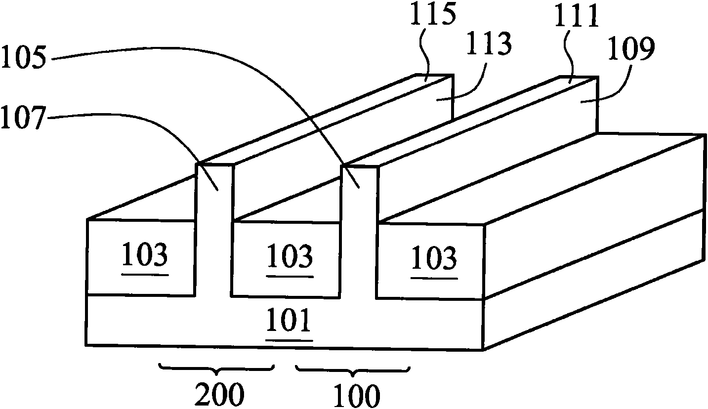
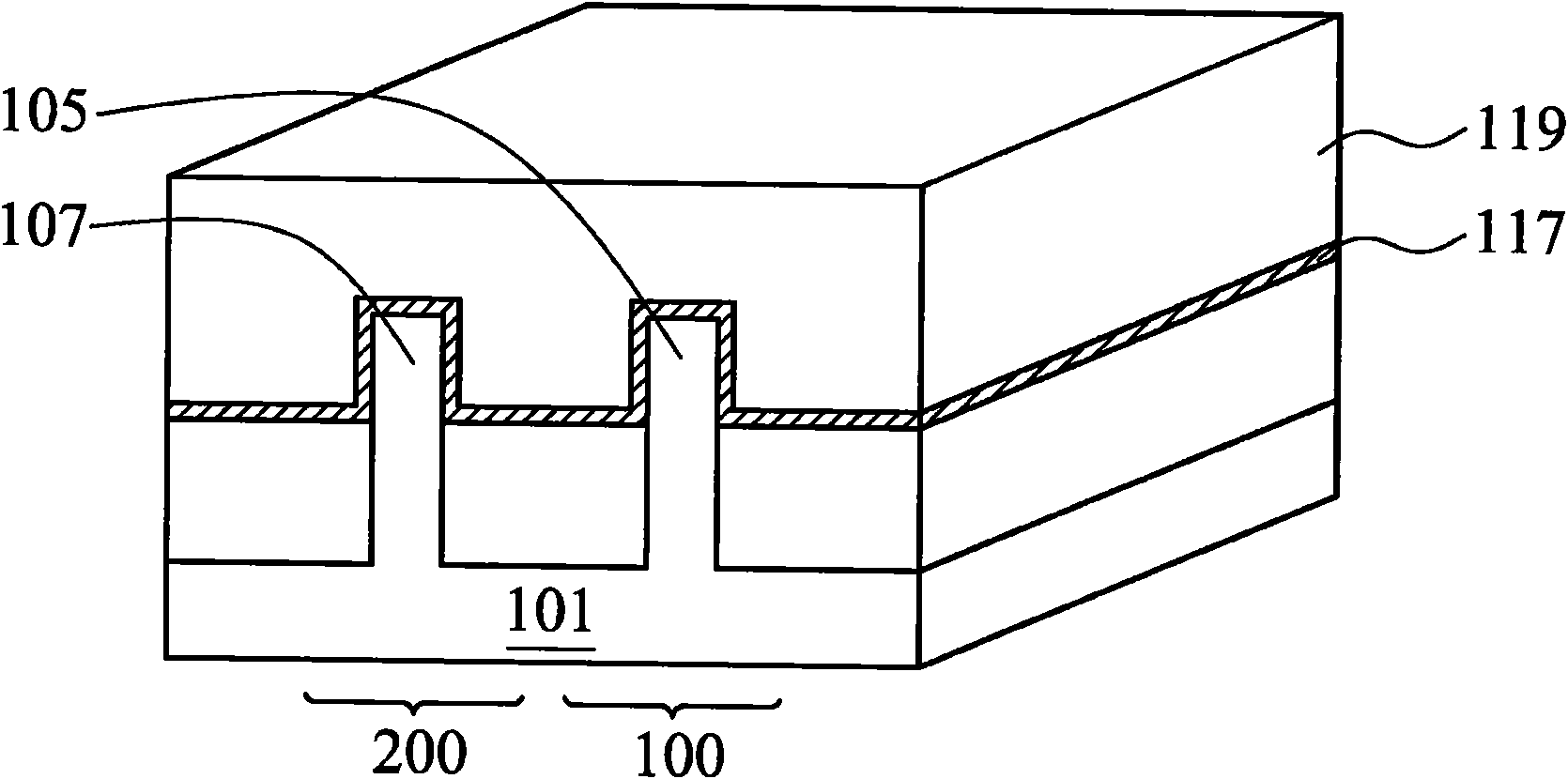
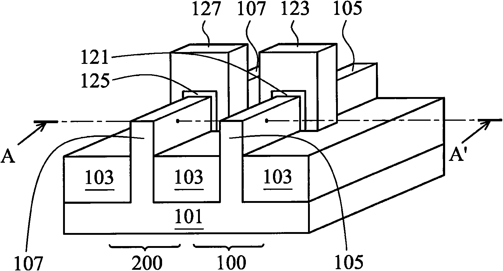
[0029] figure 1 and Figure 11 As shown, process step 501 provides a substrate including a first fin 105 and a second fin 107 . In some embodiments, the substrate 101 may be a silicon substrate, a germanium substrate or a substrate of other semiconductor materials. The substrate 101 may be doped with p-type or n-type dopants. An isolation region such as a shallow trench isolation region 103 (shallow trench isolation region, STI region) may be formed in or above the substrate 101 . The first semiconductor fin 105 and the second semiconductor fin 107 extend above the top surface of the STI region 103 . The first semiconductor fin 105 has a top surface 111 and sidewalls 109 . The second semiconductor fin 107 has a top surface 115 and side...


PUM

PropertyMeasurementUnit
Thicknessaaaaaaaaaa

Abstract

An embodiment of the disclosure includes a method for doping a FinFET (fin field-effect transistors). In the method, a dopant-rich layer comprising a dopant is formed on a top surface and sidewalls of a semiconductor fin of a substrate. A cap layer is formed to cover the dopant-rich layer. The substrate is annealed to drive the dopant from the dopant-rich layer into the semiconductor fin. Multiple embodiments of the method can improve disadvantages of traditional LDD technology. For example, in different embodiments, a dopant-rich layer and a cap layer are formed, and a tempering technology driving impurities to the LDD zone to reach the required thickness without considering shadow effect and PAI twin boundary defects is provided. Therefore, electricity of the device can be improved.

Description


Claims


Application Information

Patent Timeline
Owner TAIWAN SEMICON MFG CO LTD
Why Eureka
Try Eureka