
High voltage light emitting diode and manufacturing method thereof

A high-voltage light-emitting and diode technology, applied in the direction of semiconductor devices, electrical components, circuits, etc., can solve the problems of increasing the size and area of ​​the aluminum substrate, difficult to solve the problem of heat dissipation, and increasing the cost, so as to reduce power loss, improve efficiency and cost. reduced effect

Active Publication Date: 2013-02-13
山东聚芯光电科技有限公司
View PDF5 Cites 0 Cited by
  • Summary
  • Abstract
  • Description
  • Claims
  • Application Information

AI Technical Summary

Problems solved by technology

[0003] Because the existing diodes use low-voltage chips, the working voltage is about 3V, and the current of the 1W diode is 350 mA. The current is too large, and the problem of heat dissipation is difficult to solve. In order to quickly dissipate the heat, the size and area of ​​the aluminum substrate are often increased. It also increases its cost, and the high cost is now unaffordable for ordinary people, which affects its promotion

Method used


Image

  • High voltage light emitting diode and manufacturing method thereof
  • High voltage light emitting diode and manufacturing method thereof
  • High voltage light emitting diode and manufacturing method thereof

Examples


Embodiment

[0026] Below, the present invention will be described in detail in conjunction with the accompanying drawings.

[0027] Process the ceramic substrate first:

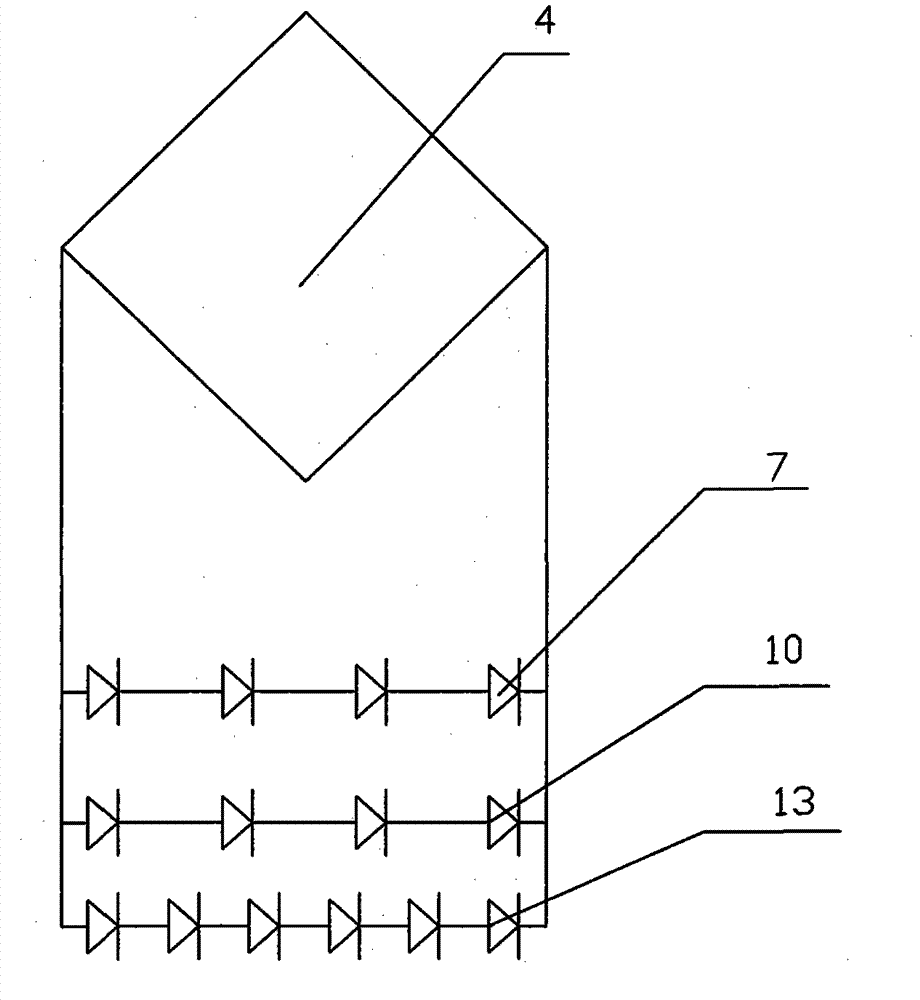
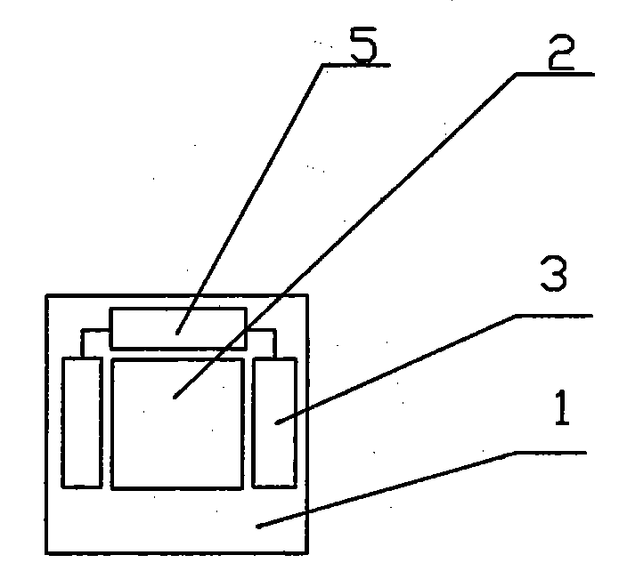
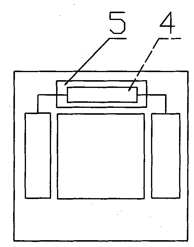
[0028] figure 1 It is a schematic diagram representing the present invention, based on the principle figure 1 , the ceramic substrate 1 is a square with a side length of 16 mm. According to the conventional process, an inner groove 2 with a side length of 8 mm is processed on the ceramic substrate 1, and the position of the bridge resistance groove 5 is reserved on the ceramic substrate 1. According to the principle figure 1 According to the requirements, the upper external electrode 3 and its leads are made on the ceramic substrate 1, and then the bridge resistor 4 is welded in the bridge resistor slot 5. The welding of the bridge resistor 4 is completed in the 10,000-level factory building.

[0029] Die-bonding of high-voltage chips:

[0030] Use an automatic crystal bonder to bond four 1W high-voltage blue-ray chip...


PUM


Abstract

The invention discloses a high voltage light emitting diode and a manufacturing method thereof. The high voltage light emitting diode comprises a ceramic substrate, four blue light chips, four green light chips and six red light chips and is characterized in that: in a high voltage light emitting diode structure, a square groove and a bridge-type resistance slot are arranged in the middle of the square ceramic substrate. The manufacturing method comprises the following steps of: firstly, welding a bridge-type resistor in the bridge-type resistance slot; secondly, bonding the four high voltageblue light chips with voltage of 47 to 55 volts, the four high voltage green light chips with voltage of 47 to 55 volts and the six high voltage red light chips with voltage of 32 to 37 volts into the square groove by using an automatic die bonder through high heat-conductive insulating glue; after the four blue light chips, the four green light chips and the six red light chips are subjected to curing, bonding golden wires to the four blue light chips, the four green light chips and the six red light chips by using an automatic wire bonder, namely connecting the four high voltage blue light chips in series, connecting the four high voltage green light chips in series and connecting the six high voltage red light in series, and connecting the three series circuits in parallel; connecting both ends of the parallel circuit to electrodes; and thirdly, uniformly stirring silica gel 6301 and coating the silica gel 6301 in the square groove, wherein the silica gel is slightly bubbled to overflow and quickly transmitted into an oven for curing, so that the high voltage light emitting diode which has a good radiating effect and low manufacturing cost and is suitable for batch production is obtained.

Description

technical field [0001] The invention relates to a light emitting diode. Background technique [0002] The use of light-emitting diodes is becoming more and more extensive. From the original indicator lights, it is developing into household lighting, and its energy-saving and environmental protection effects are remarkable. [0003] Because the existing diodes use low-voltage chips, the working voltage is about 3V, and the current of the 1W diode is 350 mA. The current is too large, and the problem of heat dissipation is difficult to solve. In order to dissipate the heat quickly, the size and area of ​​the aluminum substrate are often increased. Increased its cost again, the high cost, common people can't afford it now, affects its popularization. [0004] The problem of diode heat dissipation is a problem in the world today. How to reduce the heat of diodes during operation, improve light efficiency, and how to reduce costs have become the most concerned issues today. Con...

Claims


Application Information

Patent Timeline
Patent Type & Authority Patents(China)
IPC IPC(8): H01L25/075H01L33/48H01L33/64H01L33/00
CPCH01L2224/48091H01L2224/48137H01L2224/49113H01L2924/00014
Inventor 叶向东吉爱华汪英杰孙晖
Owner 山东聚芯光电科技有限公司
Learn More