
Method for forming thin film pattern and flat panel display having same

一种平板显示器、薄膜图案的技术,应用在形成薄膜图案以及具有该薄膜图案的平板显示器领域,能够解决难形成分辨率薄膜图案等问题

Active Publication Date: 2011-12-14
LG DISPLAY CO LTD
View PDF6 Cites 2 Cited by
  • Summary
  • Abstract
  • Description
  • Claims
  • Application Information

AI Technical Summary

Problems solved by technology

[0006] Therefore, it is difficult to form a thin film pattern with a resolution lower than the minimum line width of the thin film pattern

Method used


Image

  • Method for forming thin film pattern and flat panel display having same
  • Method for forming thin film pattern and flat panel display having same
  • Method for forming thin film pattern and flat panel display having same

Examples


Embodiment Construction

[0029] Reference will now be made in detail to specific embodiments of the invention, examples of which are illustrated in the accompanying drawings. Wherever possible, the same reference numbers will be used throughout the drawings to refer to the same or like parts.

[0030] Figures 1A-1G There are shown cross-sectional views illustrating steps of a method of forming a thin film pattern according to a preferred embodiment of the present invention.

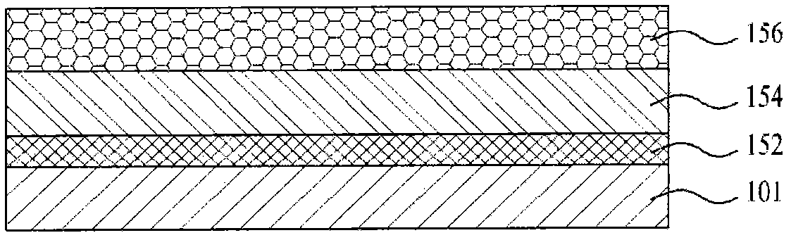
[0031] refer to Figure 1A , the first to third film layers 152 , 154 and 156 are sequentially stacked on the substrate 101 .

[0032] The first thin film layer 152 , which is a material layer of a thin film pattern to be formed on the substrate 101 , is formed of a metal, an insulating film, or a semiconductor layer.

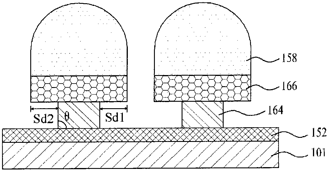
[0033] The second thin film layer 154 is formed of a material that forms an obtuse or right angle θ after the etching process. In detail, the second thin film layer 154 is formed of an inorganic insulating fil...


PUM

PropertyMeasurementUnit
widthaaaaaaaaaa

Abstract

The present disclosure is a method for forming a thin film pattern to form a micron-pattern and a flat display device having the same. The method for forming a thin film pattern includes the steps of forming first to third thin film layers on a substrate in succession, forming a first photoresist pattern on the third thin film layer, patterning the second and third thin film layers using the first photoresist pattern as a mask to form first and second thin film mask pattern having line widths different from each other, forming a second photoresist pattern at a region where the first and second thin film mask patterns do not overlap positioned between the first thin film layer and the second thin film mask pattern, removing the first and second thin film mask patterns, and patterning the first thin film layer using the second photoresist pattern as a mask.

Description

[0001] This application claims priority from Korean Patent Application No. 10-2010-0055335 filed on Jun. 11, 2010, the entire contents of which are hereby incorporated by reference. . technical field [0002] The present invention relates to a method of forming a thin film pattern capable of forming micropatterns and a flat panel display having the thin film pattern. Background technique [0003] Recently, the display market is rapidly changing centering on flat panel displays that enable easy manufacture of lightweight, large-sized displays. [0004] As the flat panel display, there are a liquid crystal display LCD, a plasma display panel PDP, an organic electroluminescence display OLED, and the like. A plurality of thin film patterns in the flat panel display are formed through a thin film deposition step, a photolithography step including exposure and development steps, and a masking step including an etching step and a photoresist removal step. [0005] The photoresist...

Claims


Application Information

Patent Timeline
Patent Type & Authority Applications(China)
IPC IPC(8): H01L21/02H01L21/77
CPCH01L27/1214H01L27/1288H01L27/12Y10T428/24802
Inventor 金正五李正一金江一方政镐白正善
Owner LG DISPLAY CO LTD
Features
  • Generate Ideas
  • Intellectual Property
  • Life Sciences
  • Materials
  • Tech Scout
  • Unparalleled Data Quality
  • Higher Quality Content
  • 60% Fewer Hallucinations
Learn More