Electrode for high-voltage in-situ impedance spectroscopy measurement and its preparation method and application

A technology of impedance spectroscopy and electrodes, applied in the field of in-situ measurement of electrical quantities, to achieve the effect of solving the insulation of the sample cavity

Inactive Publication Date: 2011-12-21
JILIN UNIV
View PDF4 Cites 16 Cited by
  • Summary
  • Abstract
  • Description
  • Claims
  • Application Information

AI Technical Summary

Benefits of technology

In this new technique called AC Impedence Spectroscopy (ACS), which was developed by Chinese scientists during their researches for materials science, there are technical improvements over previous methods such as electron beam lens micrograph analysis or atomic force microscope techniques used earlier. These improved measurements allow us to study how different types of matter behave differently when subjected to very large electric fields without affecting any other things nearby.

Problems solved by technology

This patented describes different ways to measure material's electric characteristics during high pressures without having to manually attach or connect external devices like resistors or inductive couplers onto the surface being measured. These techniques require precise placement of both elec trodes inside the device while still achieving complete isolation between them. Additionally, current methods involve injecting AC signals through conductor assemblies connected by cables, making it challenging to achieve accurate measurements due to factors such as temperature variations and magnetic field interference caused by strong alternations at frequencies near 500 kHz.

Method used


Image

  • Electrode for high-voltage in-situ impedance spectroscopy measurement and its preparation method and application
  • Electrode for high-voltage in-situ impedance spectroscopy measurement and its preparation method and application
  • Electrode for high-voltage in-situ impedance spectroscopy measurement and its preparation method and application

Examples


Embodiment 1

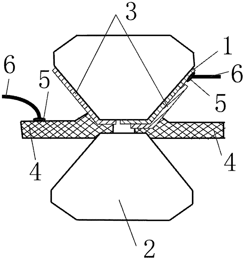
[0025] The whole device of the present invention is as figure 1 shown. Among them, 1 is a metal film electrode, 2 is a diamond anvil, 3 is an aluminum oxide protective layer, 4 is a metal gasket, 5 is a copper wire wire, and 6 is a silver paste.

[0026] The metal film electrode 1 is deposited on the anvil surface and the side surface of the diamond anvil 2, and the metal film electrode 1 is circular at one end of the anvil surface of the diamond anvil 2, and is not covered by the aluminum oxide protective layer 3; One end of the side of the anvil 2 uses silver paste 6 to bond the copper wire conductor 5 .

[0027] Metal pad 4 is used as another electrode, and silver paste 6 is also used to bond copper wire 5 .

[0028] The metal gasket 4 and the metal film electrode 1 form an axisymmetric electrode system; the two electrodes are at the sample cavity so that all the detection signals are transmitted through the sample,

Embodiment 2

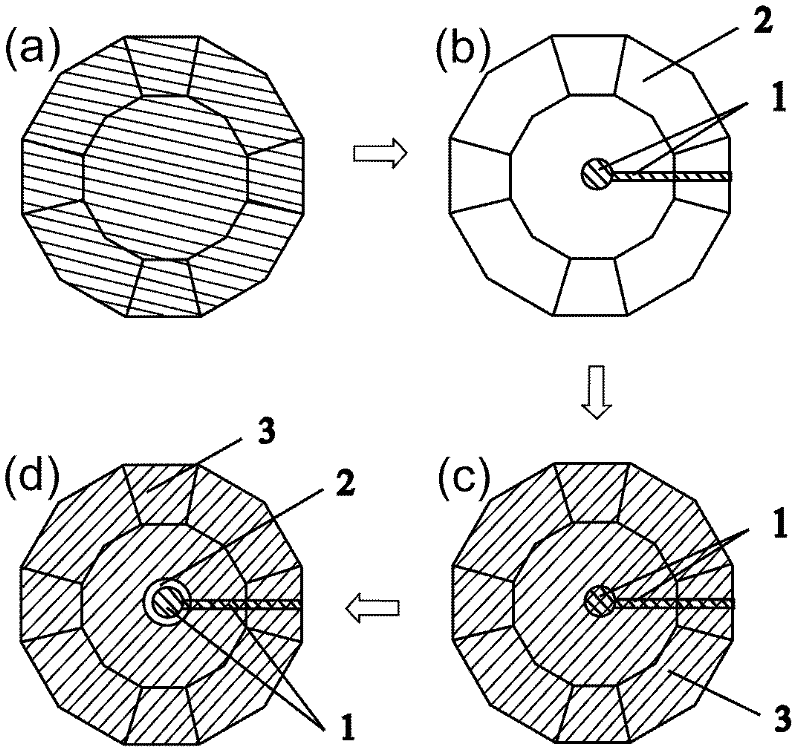
[0030] The present invention adopts following technological process [whole process is as figure 2 Shown in (a)~(d)]:

[0031] Step 1: Soak the diamond anvil in a mixed solution of acetone and alcohol (volume ratio 1:1) for 20 minutes to remove surface stains, and rinse the residual solution on the surface with deionized water after taking it out.

[0032] The second step: on the surface of the diamond anvil, a layer of metal film is plated by magnetron sputtering as an electrode material [such as figure 2 (a)]. During the sputtering process, the substrate temperature is kept at 250-300 degrees Celsius, metal materials are used as the target material, argon is used as the working gas, and the pressure in the vacuum chamber is always kept within the range of 0.8-1Pa.

[0033] Step 3: Take out the diamond anvil coated with the metal film, apply a layer of photoresist evenly on its surface, use photolithography technology to carve the shape of the electrode on the diamond anvi...

Embodiment 3

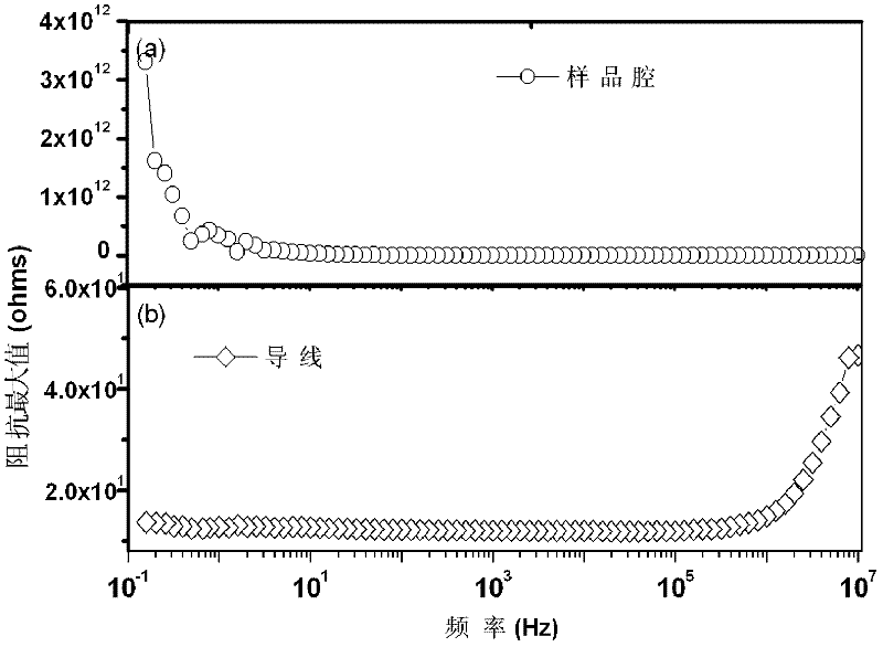
[0038] Using the electrode model designed by the invention, the impedance spectrum measurement is carried out on the nanometer ZnS. The instrument used in the experiment is a Solartron frequency response analyzer, the instrument model is 1260+1296. During the measurement, the two connection terminals are respectively connected to two thin copper wires. The input and output frequency range of the AC signal used is 10MHz-10μHz, and the amplitude of the AC voltage signal needs to be selected according to different samples. For the sample of nano-ZnS, the AC signal voltage used by the author is 0.1V.

[0039] The specific electrical quantity measurements and their results are as follows.

[0040] 1. Measurement results of parasitic capacitance and inductance of the system

[0041] Parasitic capacitance generally refers to the capacitance characteristics of inductors, resistors, chip pins, etc. under high frequency conditions. In fact, a resistor is equivalent to a capacitor, an ...


PUM


Abstract

The electrode for high-voltage in-situ impedance spectroscopy measurement of the present invention and its preparation method and application belong to the technical field of in-situ measurement of electrical quantities under high-voltage conditions. The electrode consists of an aluminum oxide protective layer (3) deposited on the surface of the diamond anvil (2) and a metal film electrode (1); the metal film electrode (1) is circular in the center of the anvil surface of the diamond anvil (2), Copper wire (5) is bonded to the metal film electrode (1) on the side of the diamond anvil (2); the metal spacer (4) is used as another electrode, forming an axisymmetric electrode together with the metal film electrode (1) system. Electrodes are prepared by magnetron sputtering, molybdenum coating, aluminum oxide deposition, photolithography and chemical corrosion. The invention solves the problems of electrode fixing and sample cavity insulation, and can ignore the influence of the parasitic capacitance and inductance of the system on the measurement results, making it possible to measure the material impedance spectrum in situ with the diamond anvil under high pressure.

Description


Claims


Application Information

Patent Timeline
Owner JILIN UNIV
Why Eureka
Try Eureka