
Frequency calibration circuit of active RC (Resistor-Capacitor) filter
A technology of frequency calibration and filter, which is applied in the field of frequency calibration circuit of active RC filter, can solve the problem of active RC filter cut-off frequency drift, etc., and achieve the effect of preventing the influence of the circuit
- Summary
- Abstract
- Description
- Claims
- Application Information
AI Technical Summary
Problems solved by technology
Method used
Image

Examples
Embodiment Construction
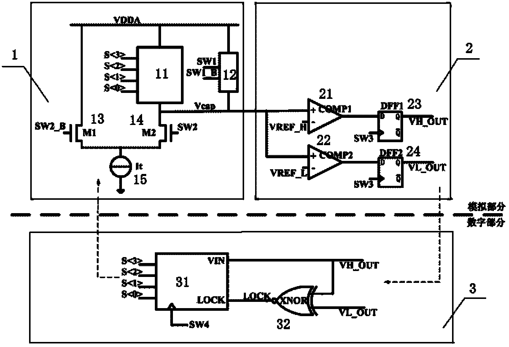
[0015] Such as figure 1 Shown is a schematic structural diagram of the frequency calibration circuit of the active RC filter of the present invention. Its structure includes a capacitor array charging and discharging circuit module 1 of the analog part, a voltage window comparison circuit module 2 and a capacitor array control signal feedback circuit module 3 of the digital part.
[0016] The capacitor array charging and discharging circuit module 1 includes a capacitor array 11, a transmission gate 12, an NMOS switch tube M113, an NMOS switch tube M214, and a tail current source It15, wherein the positive terminal of the capacitor array 11 is connected to a power line, and has a capacitance control word S, S, S, S; the negative end of the tail current source It15 is grounded; the sources of the NMOS switch M113 and the NMOS switch M214 are connected, and connected to the positive end of the tail current source It15 The gate of the NMOS switch M113 is connected to the reverse...
PUM
 Abstract
Description
Claims
Application Information