Integrated circuit, device and manufacture method thereof

A manufacturing method and circuit technology, applied in the field of integrated circuits, devices and their manufacturing, can solve the problems of lower layout efficiency, inability of inductive amplifiers to cooperate with memory cell structures, and slow reading speed of high-density memory arrays, etc., so as to reduce bit line load , Reduce the effect of reading access time

Active Publication Date: 2014-01-01
TAIWAN SEMICON MFG CO LTD
View PDF3 Cites 0 Cited by
  • Summary
  • Abstract
  • Description
  • Claims
  • Application Information

AI Technical Summary

Problems solved by technology

[0019] In the known art, one known way to shorten the number of bitline swings is to add extra sense amplifiers to each column and divide the bitline into multiple segments; however, this method reduces the layout efficiency obtained, which This is because the added sense amplifiers do not fit into the neat cell structure defined by the cell gap height, so although there is some speed benefit in terms of bitline swing times, when using these separate bitlines, the additional silicon The disadvantages created by the area penalty are undesirable
[0020] In typical known memory devices, the long bit lines caused by the memory architecture of high-density memory arrays greatly increase the time required for memory read access
Causes the read speed of high-density storage arrays to become undesirably slow
These problems continue to increase as memory array densities (number of bits) increase

Method used


Image

  • Integrated circuit, device and manufacture method thereof
  • Integrated circuit, device and manufacture method thereof
  • Integrated circuit, device and manufacture method thereof

Examples


Embodiment Construction

[0059] The manufacture and use of this preferred embodiment are discussed in detail below. It should be understood that although the present invention provides inventive concepts that can be applied in a wide variety of specific contexts. The specific embodiments discussed are merely illustrative of specific ways to make and use the invention, and do not limit the scope of the invention.

[0060] The embodiments of the present invention described in detail now provide novel circuits and methods for high-density memory arrays. Using these embodiments can reduce bit line loading without corresponding silicon area penalty, thereby reducing the read access time of the memory cell.

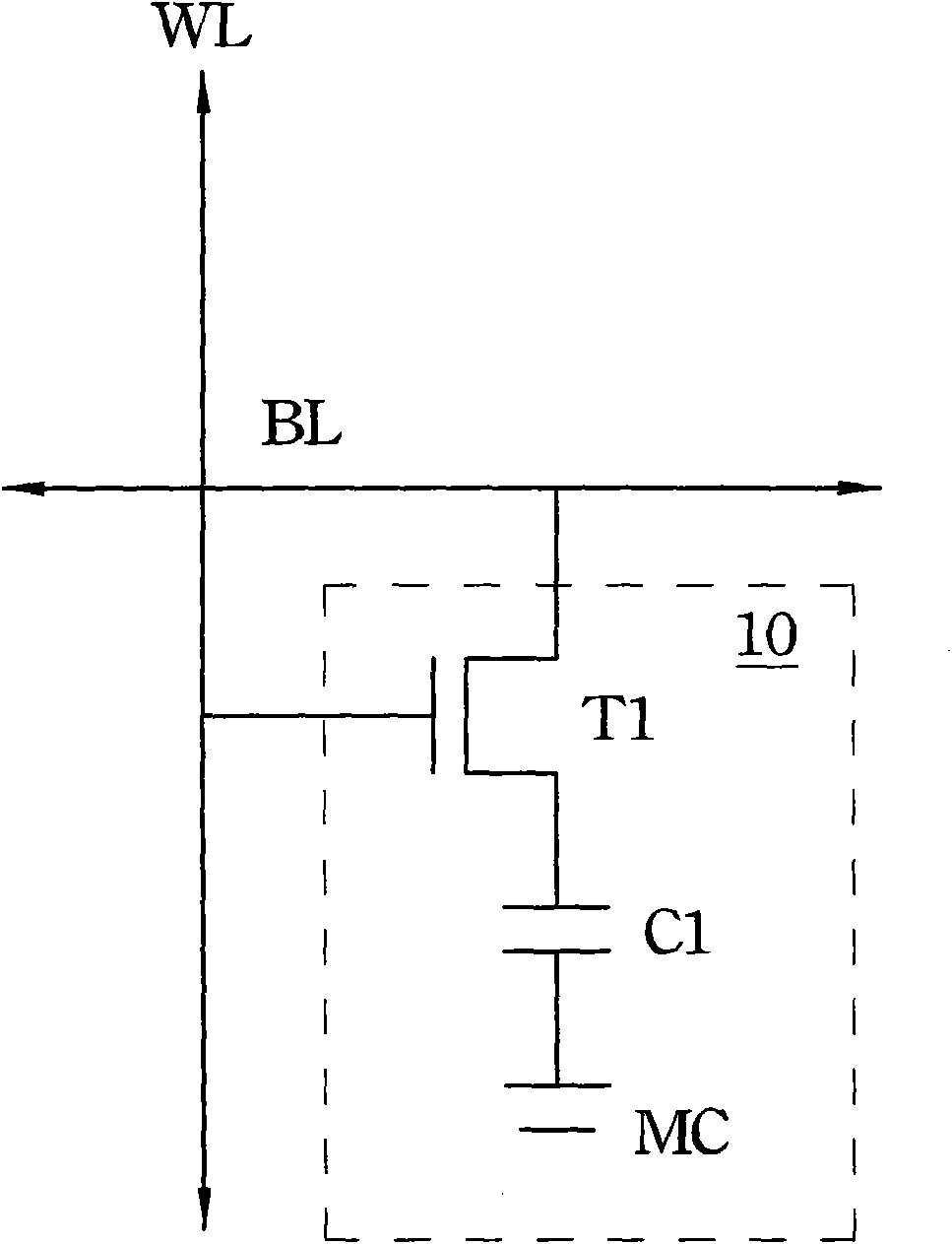
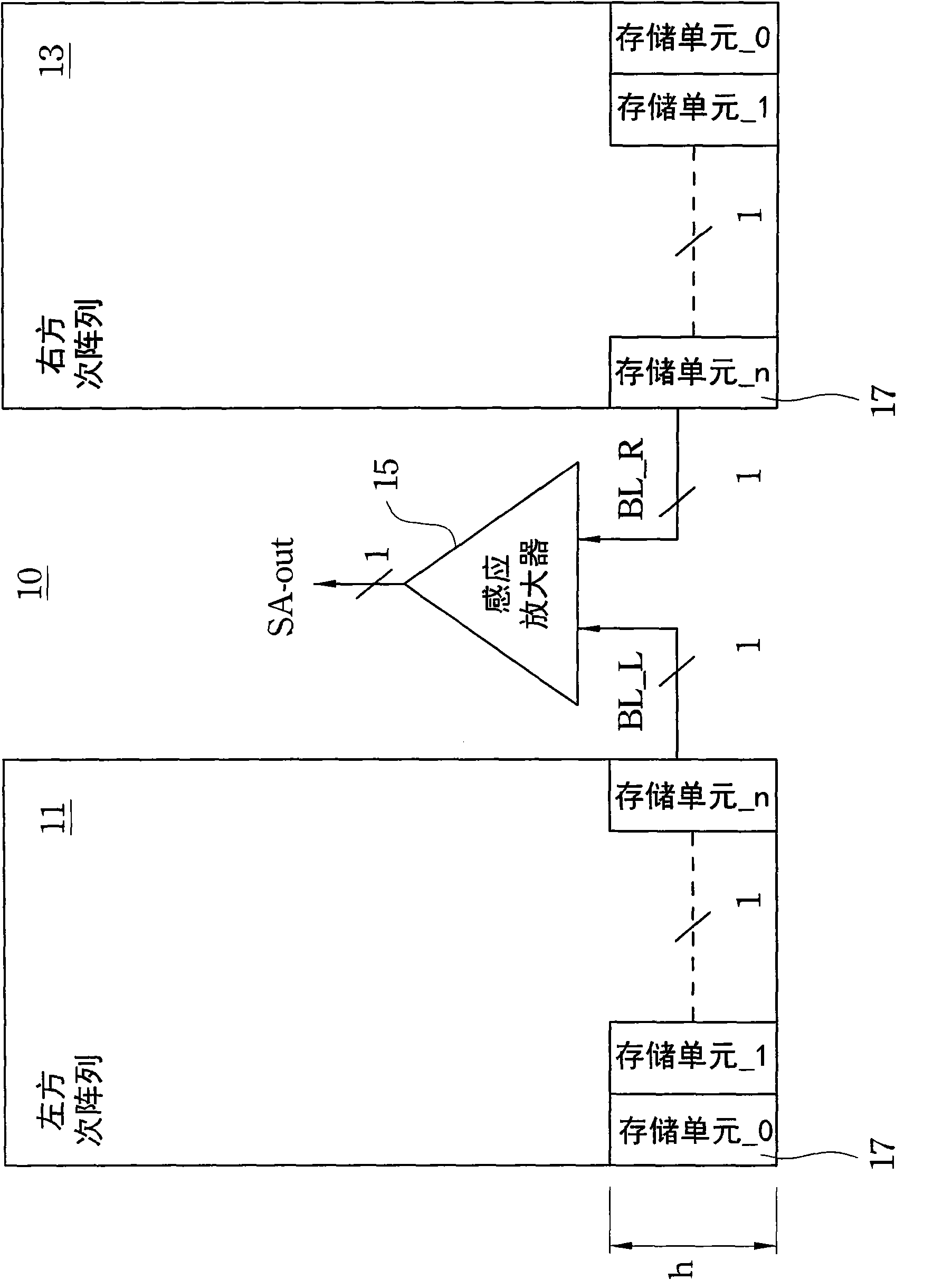
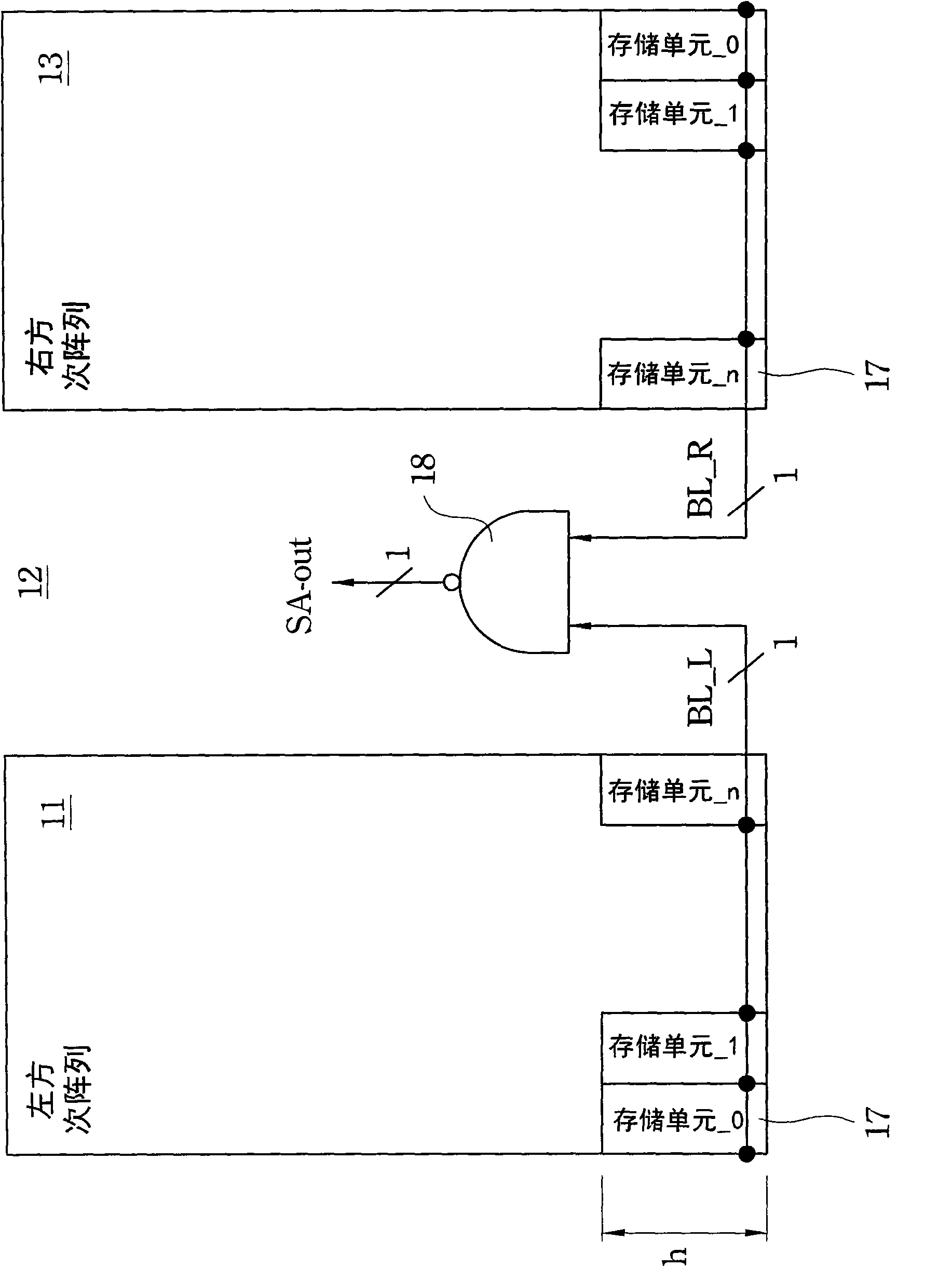
[0061] Figure 4 The storage array 40 of the first exemplary embodiment is shown. The left sub-array 51 and the right sub-array 53 are shown therein. In each array, a plurality of adjacent memory cells 17 are arranged in columns. Although not shown, examples of each memory cell column, bit lines BL_L an...


PUM


Abstract

Apparatus and methods for providing a high density memory array with reduced read access time are disclosed. Multiple split bit lines are arranged along columns of adjacent memory bit cells. A multiple input sense amplifier is coupled to the multiple split bit lines. The loading on the multiple split bit line is reduced, and the corresponding read speed of the memory array is enhanced over the prior art. The sense amplifier and the memory bit cells have a common cell pitch layout height so that no silicon area penalty arises due to the use of the multiple split bit lines and sense amplifiers. Increased memory array efficiency is achieved.

Description

Technical field [0001] The present invention relates to the use of bit lines in memory devices, such as memory devices used in integrated circuits. The bit line is coupled to the small-signal sense amplifier, and is used to receive data stored in memory cells (Memory Cells), such as stored charges. In the small-signal sense amplifier, the signal is amplified to the maximum signal level ( Full Signal Level) and output for use by integrated circuits or other circuits in the system. Background technique [0002] In the semiconductor process, for circuits manufactured by advanced electronic circuits and circuits manufactured by integrated circuits (ICs), the current general requirement is to use embedded or discrete memory devices. More and more such storage devices are provided as part of integrated circuits or a macro (Macro) and other circuits, such as user-defined logic circuits, microprocessors, microcontrollers, digital signal processors Such devices are manufactured together...

Claims


Application Information

Patent Timeline
Patent Type & Authority Patents(China)
IPC IPC(8): G11C11/4063G11C11/4091G11C11/4097
CPCG11C11/4097G11C5/063
Inventor 陈彝梓罗彬豪赖蔡兴陈佩蕙谢豪泰
Owner TAIWAN SEMICON MFG CO LTD
Why Eureka
Try Eureka