Tracking Circuit for Reducing Faults in a Memory

Active Publication Date: 2010-09-30
AVAGO TECH INT SALES PTE LTD
View PDF5 Cites 26 Cited by
  • Summary
  • Abstract
  • Description
  • Claims
  • Application Information

AI Technical Summary

Benefits of technology

[0005]Illustrative embodiments of the present invention provide techniques for advantageously reducing certain timing delay faults, incorrect data faults, and/or leakage current related faults which may occur when reading memory cells in a memory circuit. To accomplish this, embodiments of the invention include means for supplying a prescribed amount of current to a bit line corresponding to a selected memory cell for supplementing current lost on the bit line through leakage or other mechanisms. Embodiments of the invention accomplish fault prevention by delaying application of the suppleme

Problems solved by technology

Unfortunately, leakage current from the memory cells and/or other circuit elem

Method used


Image

  • Tracking Circuit for Reducing Faults in a Memory
  • Tracking Circuit for Reducing Faults in a Memory
  • Tracking Circuit for Reducing Faults in a Memory

Examples


Example

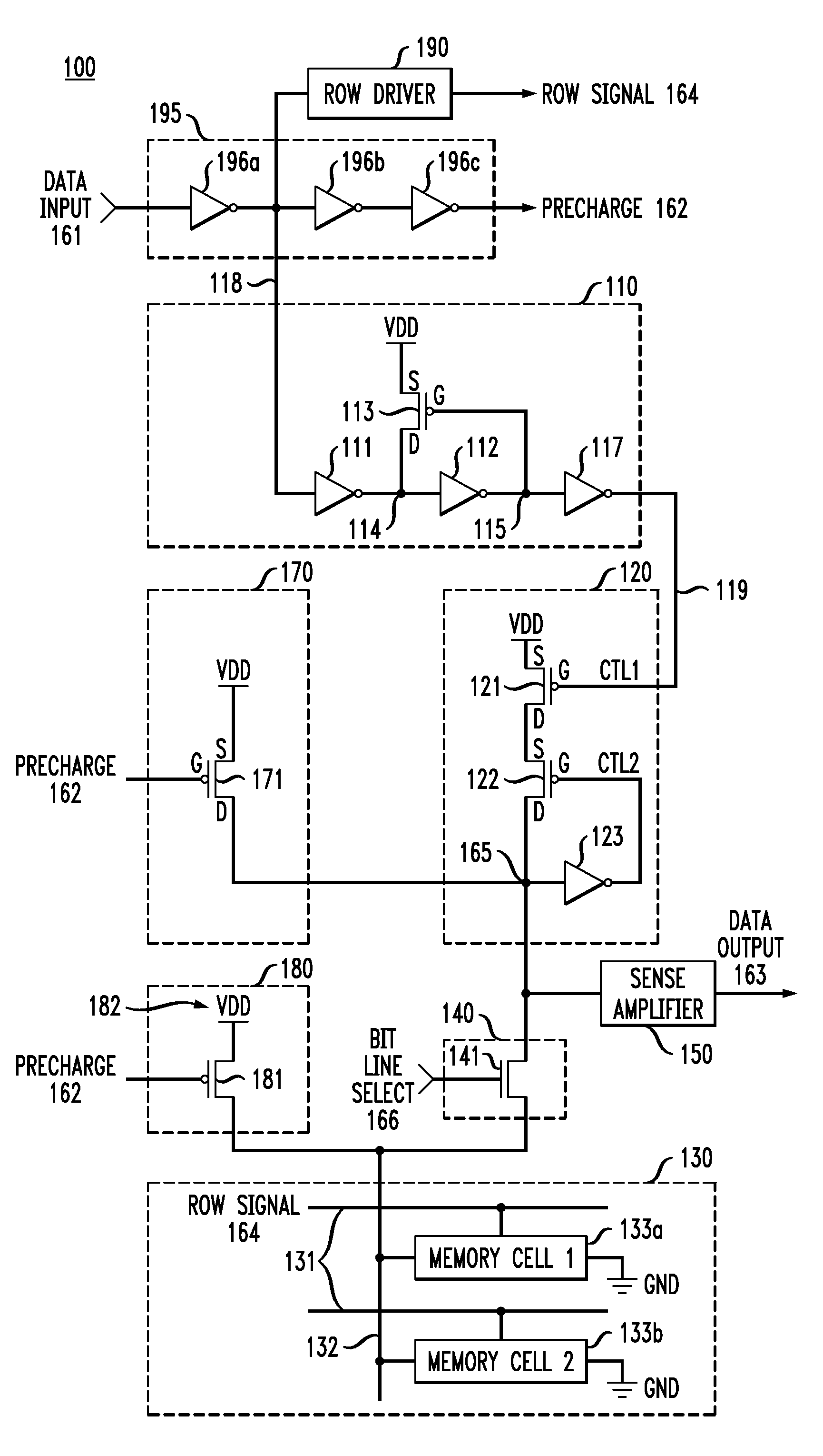
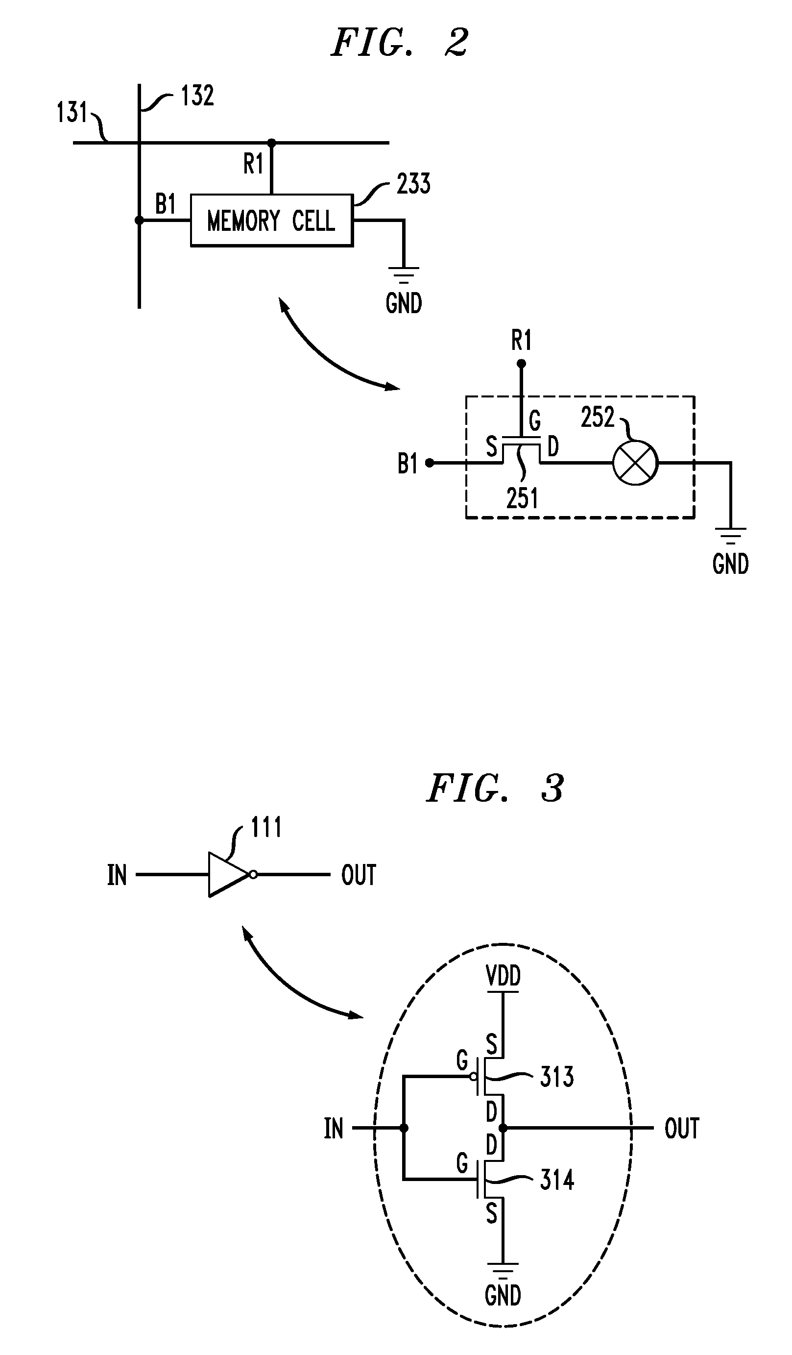
[0017]The present invention will be described herein in the context of illustrative embodiments of a memory circuit and method for accessing a memory cell in a memory circuit. It is to be appreciated, however, that the techniques of the present invention are not limited to the specific circuits and method shown and described herein. Rather, embodiments of the invention are directed broadly to improved techniques for accessing and for sensing data in a memory circuit. For this reason, numerous modifications can be made to the embodiments shown and the results will still be within the scope of the invention. No limitations with respect to the specific embodiments described herein are intended or should be inferred.

[0018]Although implementations of the present invention may be described herein with specific reference to n-channel metal-oxide-semiconductor (NMOS) transistors devices and p-channel metal-oxide-semiconductor (PMOS) transistor devices, as may be formed using a complementary...


PUM


Abstract

A memory circuit includes a plurality of memory cells and a plurality of bit lines and row lines connected to the memory cells for accessing selected memory cells. The memory circuit includes a programmable voltage source adapted for connection to at least one bit line and operative to precharge the bit line to a prescribed voltage level prior to accessing a selected one of the memory cells coupled to the bit line. A control circuit coupled to the bit line is operative to oppose discharge of the bit line during at least a portion of a given memory read cycle. A tracking circuit connected to the control circuit is operative to control a delay in activation of the control circuit and/or a duration of time the control circuit is active as a function of a parameter affecting signal development time of a data signal on the bit line.

Description

FIELD OF THE INVENTION[0001]The present invention relates generally to the electrical, electronic, and computer arts, and more particularly relates to memory circuits.BACKGROUND OF THE INVENTION[0002]Single-ended sensing techniques are used in many circuit applications for both memory and logic. Standard memory arrays include a plurality of row lines, often arranged horizontally, a plurality of bit lines, often arranged vertically orientation (e.g., in columns), and a plurality of memory cells, each memory cell being coupled to a unique pair of row and bit lines. A first subset of the memory cells are typically connected to a common row line. Likewise, a second subset of the memory cells, which may include memory cells from the first subset, are typically connected to a common bit line. When a given row line is activated, data states within the memory cells connected to the row line are coupled to the corresponding bit lines; typically, only one memory cell is coupled to its corresp...

Claims


Application Information

Patent Timeline
IPC IPC(8): G11C7/00
CPCG11C7/04G11C7/22G11C7/12
Inventor DUDECK, DENNIS E.EVANS, DONALD ALBERTPHAM, HAI QUANGWERNER, WAYNE E.WOZNIAK, RONALD JAMES
Owner AVAGO TECH INT SALES PTE LTD
Why Eureka
Try Eureka