Method for building MOSFET (Metal-Oxide-Semiconductor Field Effect Transistor) model

A model and global model technology, applied in special data processing applications, instruments, electrical digital data processing, etc., can solve problems such as poor accuracy, achieve fast models, good model accuracy, and eliminate parameter discontinuities

Active Publication Date: 2012-03-21
SHANGHAI HUAHONG GRACE SEMICON MFG CORP
View PDF2 Cites 3 Cited by
  • Summary
  • Abstract
  • Description
  • Claims
  • Application Information

AI Technical Summary

Problems solved by technology

But for a single device, the global model (Global Model) is not as

Method used


Image

  • Method for building MOSFET (Metal-Oxide-Semiconductor Field Effect Transistor) model
  • Method for building MOSFET (Metal-Oxide-Semiconductor Field Effect Transistor) model
  • Method for building MOSFET (Metal-Oxide-Semiconductor Field Effect Transistor) model

Examples


Embodiment Construction

[0020] In order to make the object, technical solution and advantages of the present invention clearer, the present invention will be further described in detail below in conjunction with the accompanying drawings.

[0021] The method for establishing a MOSFET model provided by the present invention combines the block model (Binning Model) and the global model (Global Model) on the basis of traditional BSIM3, and uses the global (Global) method to extract the block model (Binning Model) . The concrete steps of the method for setting up MOSFET provided by the present invention are as follows:

[0022] 1. Extract the global model (Global Model) in the entire device size array.

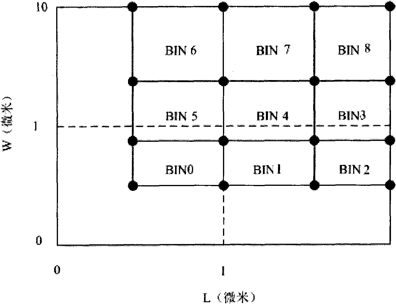
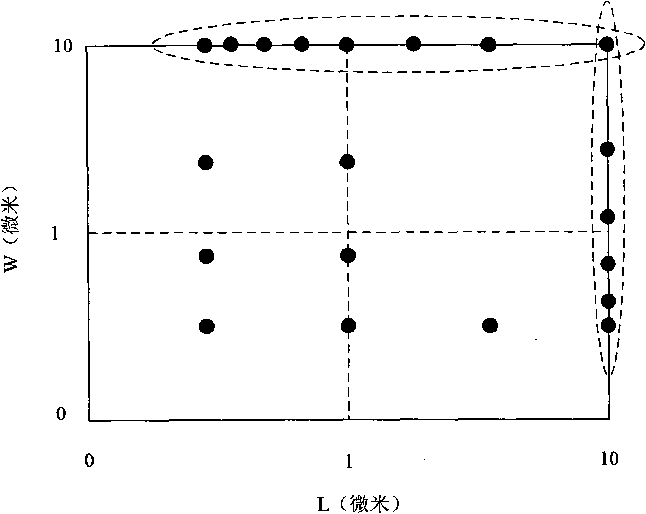
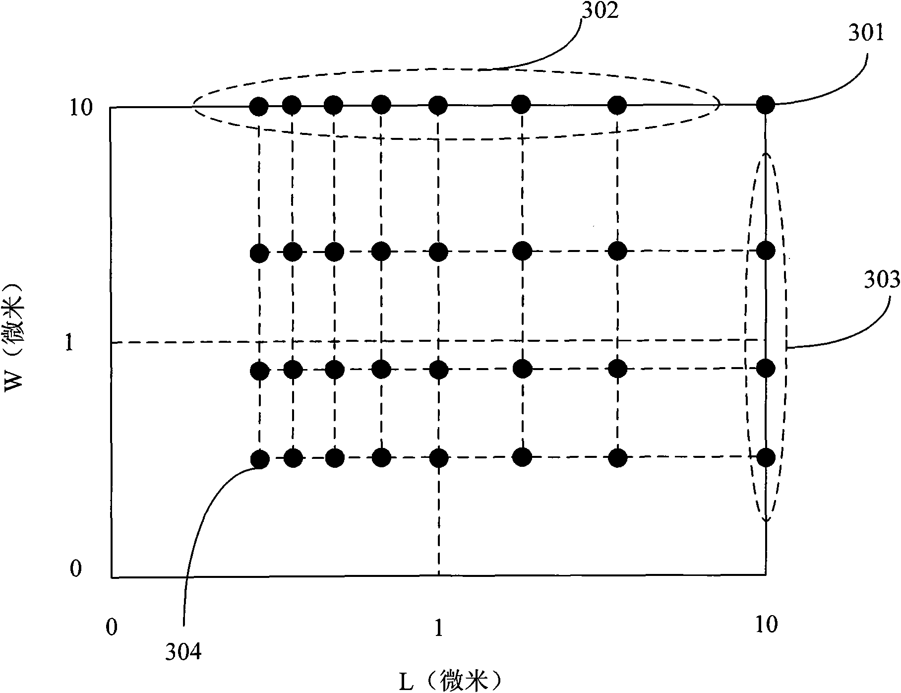
[0023] A coordinate system is established with the gate length L of the MOSFET as the abscissa and the gate width w of the MOSFET as the ordinate. A single MOSFET is represented by a point in this coordinate system, and all MOSFETs correspond to the points in this coordinate system to form a device siz...


PUM


Abstract

The invention provides a method for building a MOSFET (Metal-Oxide-Semiconductor Field Effect Transistor) model, comprising the following steps: 1. build a coordinate system by taking grid length and grid width of the MOSFET as coordinate axes and extract a global model from the whole device dimension array of the coordinate system; 2. set the parameters including Dvt0, Dvt1, Dvt2, n1x, prwg, prwb, k3, k3b, w0, dwg, dwb, b0, b1, l1, lw, lw1, ww, w1, ww1, which are in the global model and are extracted in the step one, as 0; 3. extract single models of all MOSFET devices in the device dimension array on the basis of the global model extracted in the step 2; 4. extract a blocking model. In the method, the blocking model is built by adopting a global method, the advantages of the global model and the blocking model are combined, while discontinuity of parameters is eliminated, and good model precision is achieved, and moreover, the model can be quickly built.

Description

technical field [0001] The invention relates to the field of semiconductor device models, in particular to a method for establishing a metal-oxide-semiconductor field effect transistor (MOSFET) model. Background technique [0002] With the development of the integrated circuit industry, the scale of integrated circuits is getting bigger and bigger, and the complexity is getting higher and higher. Modeling and simulating devices has become an increasingly important step in integrated circuit design. It can greatly shorten the product design and manufacturing cycle, improve efficiency, save costs, and increase yield. At present, two methods are mainly used to establish MOSFET models: one is the Binning Model method, and the other is the Global Model method. [0003] The block model (Binning Model) is generally in figure 1 Extracted from the device size array shown. In the figure, the abscissa L is the gate length of the MOSFET, and the ordinate W is the gate width of the M...

Claims


Application Information

Patent Timeline
IPC IPC(8): G06F17/50
Inventor 朱正鹏
Owner SHANGHAI HUAHONG GRACE SEMICON MFG CORP
Why Eureka
Try Eureka