High-impedance network

A high-impedance, network technology, applied in impedance networks, multi-terminal-pair networks, improving amplifiers to improve efficiency, etc., can solve problems such as limiting the low-frequency pole of the filter and limiting the signal processing quality of the filter.

Inactive Publication Date: 2012-03-21
FAIRCHILD SEMICON CORP
View PDF3 Cites 4 Cited by
  • Summary
  • Abstract
  • Description
  • Claims
  • Application Information

AI Technical Summary

Problems solved by technology

By providing a conventional filter on-chip with or near a power supply or other circuitry, the signal processing quality of the filter may be limited due to distortion caused by the power supply or other circuitry, as well as the ability of the filter to provide low frequency poles ability

Method used


Image

  • High-impedance network
  • High-impedance network
  • High-impedance network

Examples


Embodiment Construction

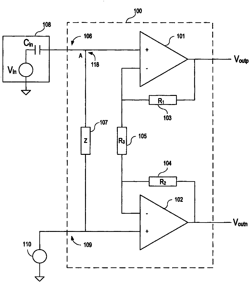
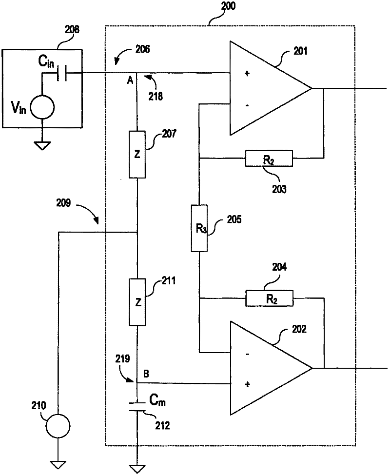
[0013] Integrated circuits have been miniaturized to accommodate the passive components associated with the circuit, including capacitors and the capacitance of those capacitors. Capacitors and impedance devices, such as resistors, may be used in filter circuits, for example to establish the poles of the filter. The poles of a filter provide an indication of the circuit's ability to pass or reject specific signal frequencies. For circuits that require low frequency poles, the reduced capacitance levels of integrated circuits require more area for capacitors or more area for larger impedance devices. The present invention develops a high impedance network for integrated circuits to provide extremely high impedance with a very small chip area. High impedance devices can be used in on-chip filter circuits with very low frequency poles. Such poles can be on the order of fractions of a Hertz. The small size of the high impedance network allows the use of integrated circuits with...


PUM


Abstract

Apparatus and methods for an integrated circuit, high-impedance network are provided. In an example, the network can include an anti-parallel diode pair coupled between first and second nodes. The anti-parallel diode pair can include a first diode including a P+/NWELL junction and a second diode including N+/PWELL junction. In an example, the first diode and the second diode can include a common substrate.

Description

technical field [0001] The subject matter of the present invention relates generally to amplifier circuits and, more particularly, to high impedance networks for amplifier circuits. Background technique [0002] Typically, a sensor circuit receives an electrical signal from a transducer. The sensor circuit then amplifies the received signal to the required level for processing. In some sensor circuits, the signal is biased and amplified to provide a differential output. Noise on the power supply, for example on the common-mode power supply used for the bias signal, may interfere with the reception and amplification of the received sensor signal. In some sensor circuits, filters are often used to pass signals with specific frequencies of interest. By providing a conventional filter on-chip with or near a power supply or other circuitry, the signal processing quality of the filter may be limited due to distortion caused by the power supply or other circuitry, as well as the...

Claims


Application Information

Patent Timeline
Patent Type & Authority Applications(China)
IPC IPC(8): H03H7/38
CPCH03F3/45475H03F2203/45138H03F3/45928H03F1/02H03F3/10H03K17/74
Inventor 安德鲁·M·乔丹哈维耶·雅撒史蒂文·M·沃斯汀
Owner FAIRCHILD SEMICON CORP
Why Eureka
Try Eureka