Manufacture method of dual-sided printed circuit board
A technology for printed circuit boards and manufacturing methods, which is applied in the fields of printed circuit manufacturing, printed circuits, electrical components, etc., and can solve problems such as easy displacement, misalignment of top and bottom PCB diagrams, and difficulty in making double-sided panels.
- Summary
- Abstract
- Description
- Claims
- Application Information
AI Technical Summary
Problems solved by technology
Method used
Image

Examples
Embodiment Construction
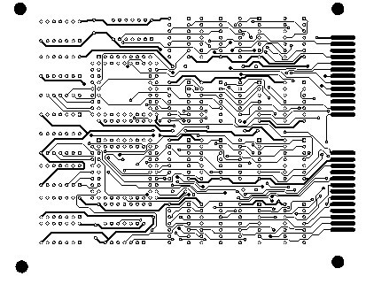
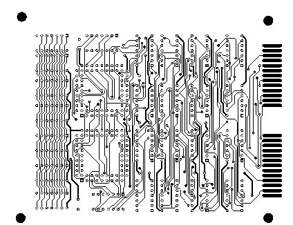
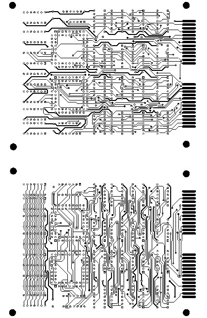
[0024] First use the printed circuit board auxiliary design software to draw the double-sided PCB diagram; then print the top PCB diagram to the electronic image file A, such as figure 1 shown; then print the bottom PCB diagram to the electronic image file B, such as figure 2 shown; then electronic picture file A and electronic picture file B are integrated into a line-symmetrical electronic picture file C, such as image 3 As shown, then print the electronic picture file C onto the thermal transfer paper; fold the thermal transfer paper along the symmetrical line, place the double-sided copper clad board in the middle of the thermal transfer paper; use the circuit board thermal transfer machine to print the top PCB pattern The printed circuit board and the bottom PCB are thermally transferred to the two sides of the double-sided copper clad laminate respectively; corrosion, drilling and some other follow-up processes will get the double-sided printed circuit board, and the c...
PUM
 Abstract
Description
Claims
Application Information
 - R&D
- Intellectual Property
- Life Sciences
- Materials
- Tech Scout
- Unparalleled Data Quality
- Higher Quality Content
- 60% Fewer Hallucinations
Browse by: Latest US Patents, China's latest patents, Technical Efficacy Thesaurus, Application Domain, Technology Topic, Popular Technical Reports.
© 2025 PatSnap. All rights reserved.Legal|Privacy policy|Modern Slavery Act Transparency Statement|Sitemap|About US| Contact US: help@patsnap.com