Manufacturing method of goldfinger circuit board

A circuit board manufacturing and gold finger technology, which is applied in the field of gold finger circuit board production, can solve problems such as short circuits and changes in electrical parameters of gold fingers, and achieve the effects of improving reliability, improving aesthetics, and avoiding short circuit phenomena.

Active Publication Date: 2013-11-27
SHENZHEN WUZHU TECH +1
View PDF5 Cites 0 Cited by
  • Summary
  • Abstract
  • Description
  • Claims
  • Application Information

AI Technical Summary

Problems solved by technology

The residue of the plating lead 13 will lead to changes in the electrical parameters of the gold finger, and even cause a short circuit due to the plating lead during the plug-in process.

Method used


Image

  • Manufacturing method of goldfinger circuit board
  • Manufacturing method of goldfinger circuit board
  • Manufacturing method of goldfinger circuit board

Examples


Embodiment Construction

[0033] Specific embodiments of the present invention will be described in detail below in conjunction with the accompanying drawings.

[0034] Before the gold finger is electroplated, it is necessary to use the electroplating lead wire to electrically connect and conduct each gold finger pattern, and then use the electroplating method to plate gold on the gold finger pattern through the electroplating lead wire, and finally form a gold finger with a gold layer.

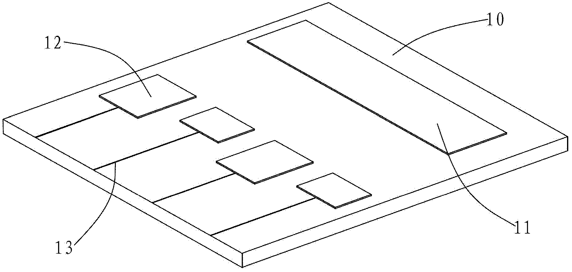
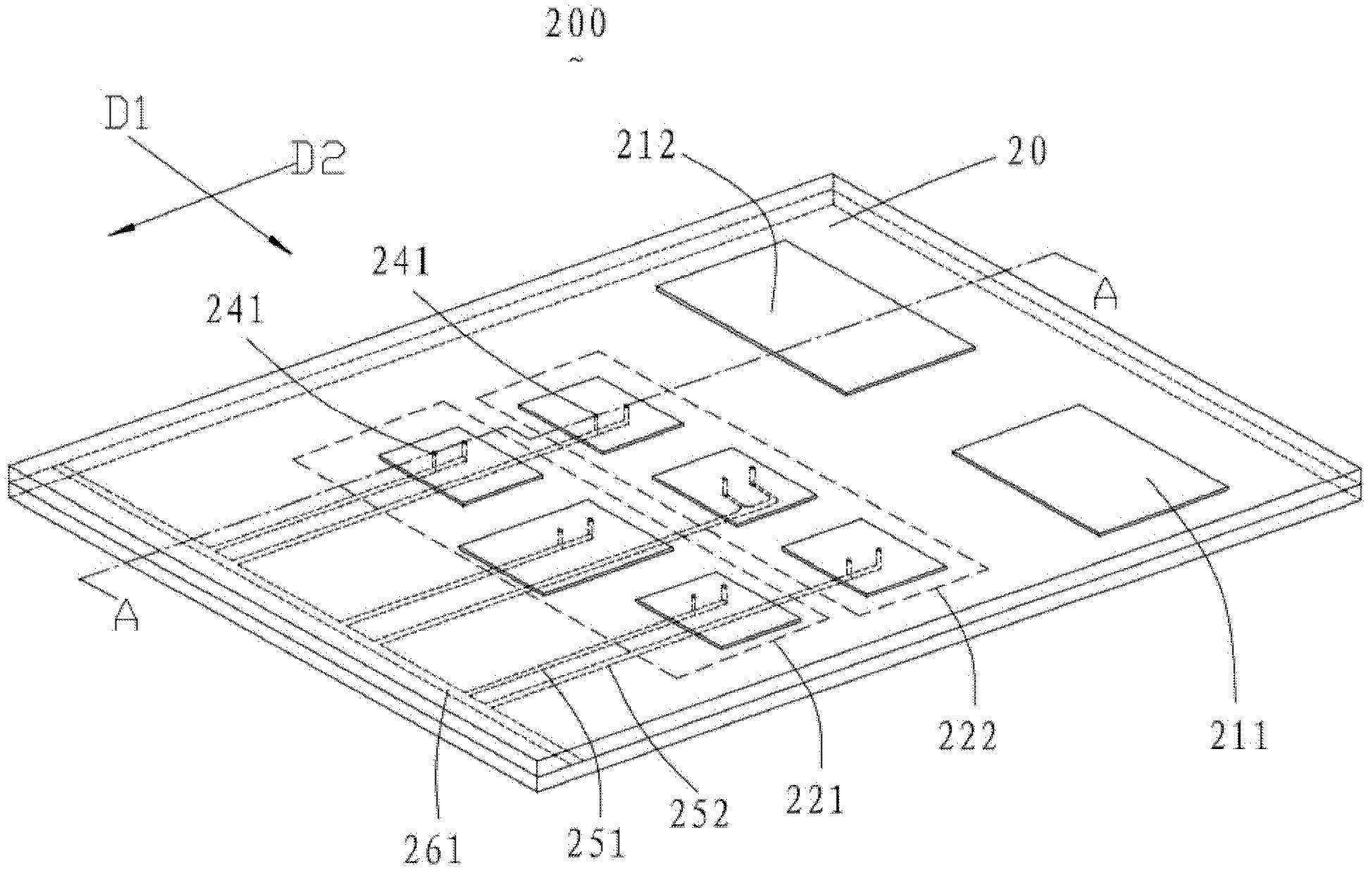
[0035] Please refer to image 3 and Figure 4 , image 3 It is a three-dimensional structural schematic diagram of the manufacturing process of the golden finger circuit board 200 according to the first embodiment of the present invention, Figure 4 for along image 3 The schematic diagram of the cross-sectional structure of line A-A is shown. The golden finger circuit board 200 includes a substrate 20 and electronic components disposed on the substrate 20 .

[0036] The substrate 20 includes a first board layer ...


PUM


Abstract

The invention relates to a manufacturing method of a goldfinger circuit board. The manufacturing method comprises the following steps of: providing a circuit board substrate with a plurality of plies, forming a plurality of groups of goldfingers on the surface of one ply, and forming a plurality of groups of electroplating leads corresponding to the plurality of groups of goldfingers on the surfaces of plies which are different from the ply where the goldfingers are located, wherein splicing directions of the plurality of groups of goldfingers are consistent and projections of the goldfingers are partially overlapped; forming a plurality of metallized copper pillars in the circuit board substrate, wherein each goldfinger is electrically connected to the corresponding electroplating lead through at least one metallized copper pillar; electroplating the goldfingers through the electroplating leads; and removing redundant circuit board substrate and electroplating leads. The goldfinger circuit board manufactured by using the circuit board manufacturing method disclosed by the invention has the advantages of attractive appearance and high electric reliability.

Description

technical field [0001] The invention relates to a method for manufacturing a circuit board, in particular to a method for manufacturing a circuit board with multiple groups of golden fingers. Background technique [0002] Printed Circuit Board (PCB) is the basis of almost any electronic product and appears in almost every electronic device. Generally speaking, if there are electronic components in a certain device, they are also integrated on PCBs of various sizes. [0003] In addition to fixing various components, the main function of PCB is to provide connection circuits between various components. As electronic equipment becomes more and more complex, more and more components are required, and the lines and components on the surface of the PCB are becoming more and more dense. [0004] Some circuit boards need to be equipped with long and short gold fingers due to the need for connection interfaces. The gold fingers are composed of many golden-yellow conductive contacts...

Claims


Application Information

Patent Timeline
Patent Type & Authority Patents(China)
IPC IPC(8): H05K3/40
Inventor 徐学军
Owner SHENZHEN WUZHU TECH
Why Eureka
Try Eureka