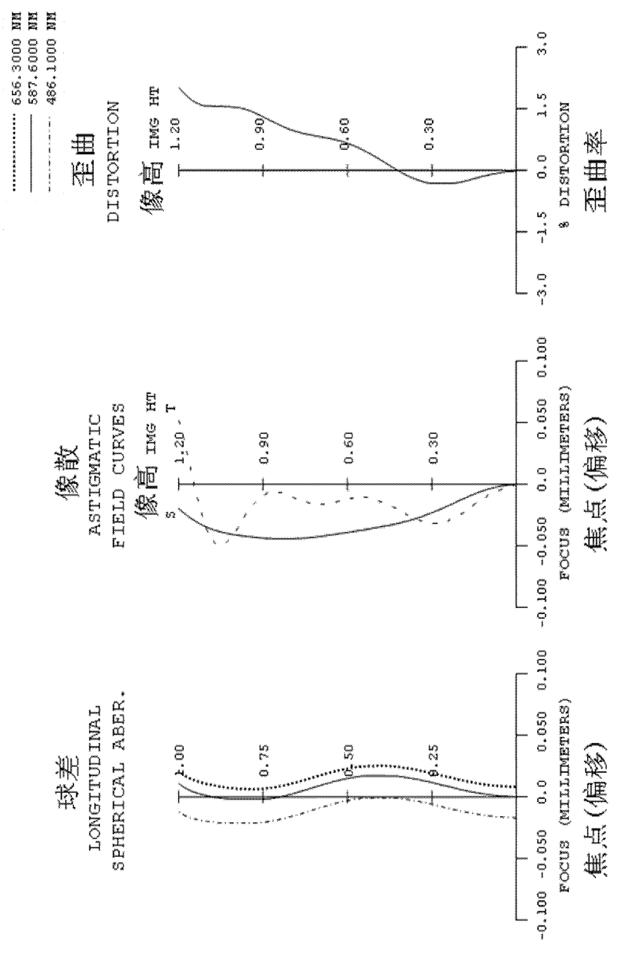
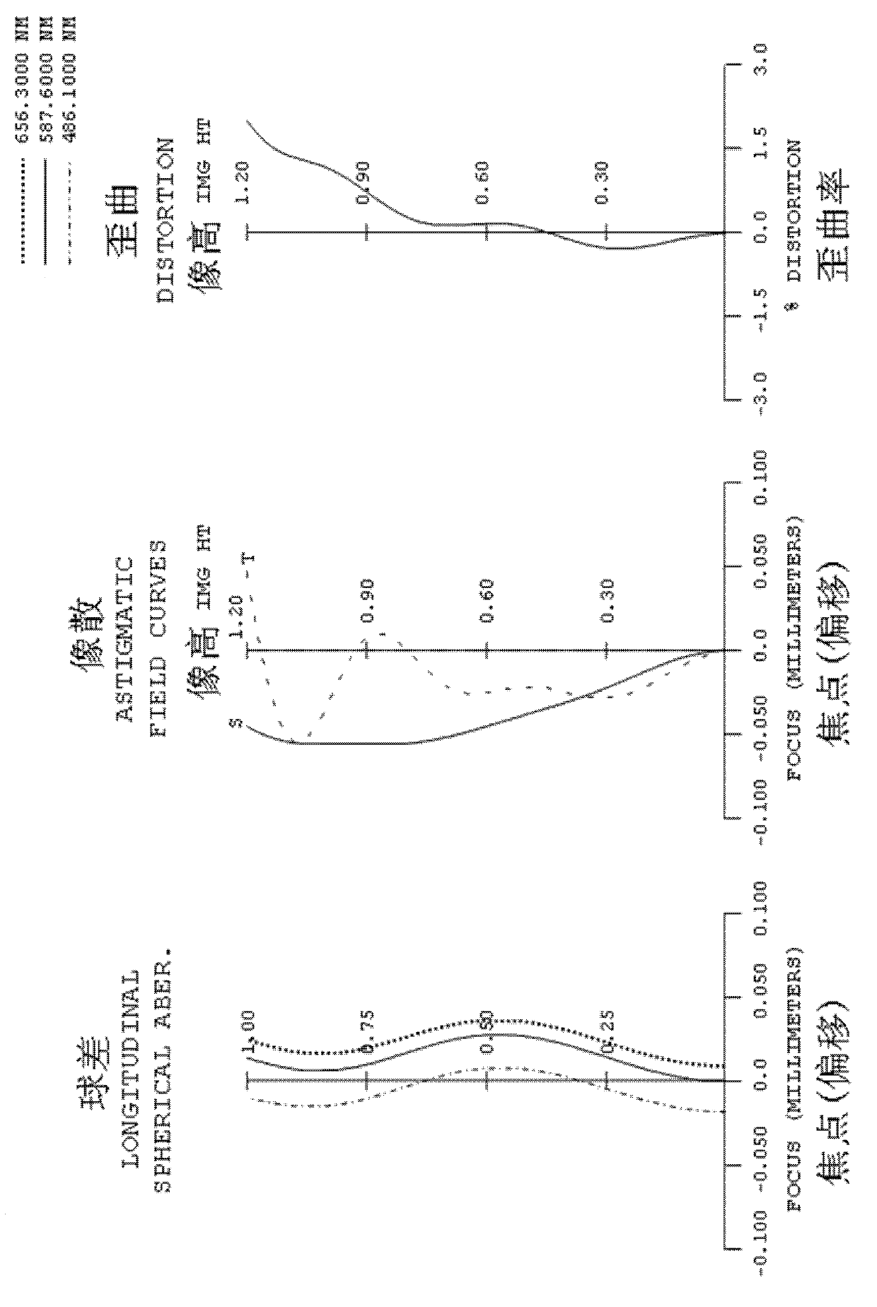
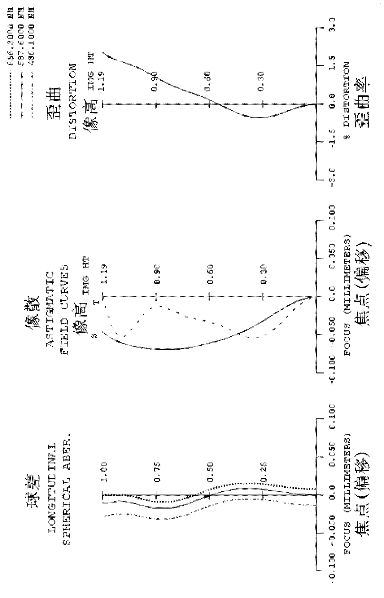
Thin type photographing lens group
A photographic lens and lens technology, applied in the direction of lenses, optics, instruments, etc., can solve problems such as inferior and significant effects, achieve high resolution, correct system aberration and astigmatism, and reduce the size of the lens
Active Publication Date: 2014-06-11
LARGAN PRECISION
View PDF2 Cites 0 Cited by
- Summary
- Abstract
- Description
- Claims
- Application Information
AI Technical Summary
Problems solved by technology
In order to correct aberrations, the form of a pre-aperture is generally used. For example, US Patent No. 7,436,604 discloses a thin camera optical mirror group composed of two lenses, but its second lens shape adopts a biconcave lens. For aberrations and Astigmatism correction, its effect is not as significant as that of the crescent lens
Method used
View moreImage
Smart ImageViewing Examples
Examples
no. 1 example
Login to View More PUM
 Abstract
The utility model discloses a thin type photographing lens group which comprises a first lens with forward refractive power and a second lens with negative refractive power, and the first lens and the second lens are arranged in sequence from an object side to an image side; the surface of the object side of the first lens is convex, the surface of the image side of the first lens is concave, and at least one of surfaces of the object side and the image side is an aspherical surface; the surface of the object side of the second lens is concave, the surface of the image side of the second lens is convex, and at least one of surfaces of the object side and the image side is of an aspherical surface; the chromatic dispersion coefficient of the first lens is V1, and the chromatic dispersion coefficient of the second lens is V2, the whole focal distance of the thin type photographing lens group is f, the focal distance of the second lens is f2, the curvature radius of the surface of the object side of the second lens is R3, the thin type photographing lens group is additionally provided with an aperture, the distance from the aperture to an optical axis of the image side is SL, and the distance from the surface of the object side of the first lens to the optical axis of the image side is TTL, which meets the following relational expressions: the absolute value of (V1-V2) is larger than 15 and smaller than 48; f / f2 is larger than minus 0.43 and smaller than 0; R3 / f is larger than minus 1.50 and smaller than minus 0.40; and SL / TTL is larger than 0.9 and smaller than 1.1. The adoption of the lens configuration manner can effectively reduce the volume of the camera, correct system aberration and astigmation, and can better obtain higher resolving power.
Description
technical field The invention relates to a photographic lens group, in particular to a miniaturized two-piece thin photographic lens group applied to electronic products. Background technique In recent years, with the increasing demand for thin photographic lenses and the improvement of semiconductor process technology, photographic lenses currently use photocoupled devices (Charge Coupled Device, CCD) or complementary metal oxide semiconductor components (Complementary Metal -Oxide Semiconductor Sensor, CMOS Sensor) photosensitive components, the pixel size can be miniaturized, and the development trend of today's electronic products is light, thin and small. Therefore, optical systems with good image quality and thin shape have become the current market. on the mainstream. In order to correct the aberrations, the traditional thin camera optical lens group mainly adopts a three-piece lens structure, the most common of which is the positive and negative positive Triplet ty...
Claims
Login to View More Application Information
Patent Timeline
 Patent Type & Authority Patents(China)
IPC IPC(8): G02B13/18G02B13/00G02B13/22G02B3/02G02B1/04G02B9/10
Inventor 谢东益蔡宗翰黄歆璇
Owner LARGAN PRECISION


