Eureka AIR delivers breakthrough ideas for toughest innovation challenges, trusted by R&D personnel around the world.

Direct welding processing method of electronic label

A technology of electronic tags and direct welding, applied in the field of RFID electronic tags, can solve the problem of high processing costs of electronic tags

Inactive Publication Date: 2012-06-27
江苏安智博电子科技有限公司
View PDF5 Cites 0 Cited by
  • Summary
  • Abstract
  • Description
  • Claims
  • Application Information

AI Technical Summary

Problems solved by technology

It is packaged by SOP technology, which can withstand external impact, but it needs to use SMT (surface mount technology) for chip patch installation, and the total processing cost of electronic tags is relatively high

Method used


Image

  • Direct welding processing method of electronic label
  • Direct welding processing method of electronic label
  • Direct welding processing method of electronic label

Examples


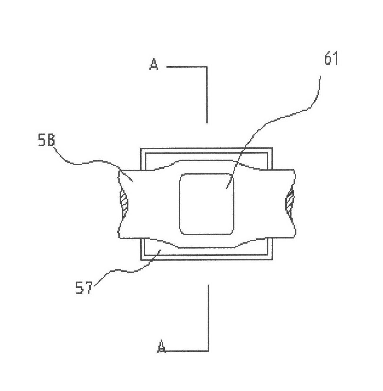
Embodiment Construction

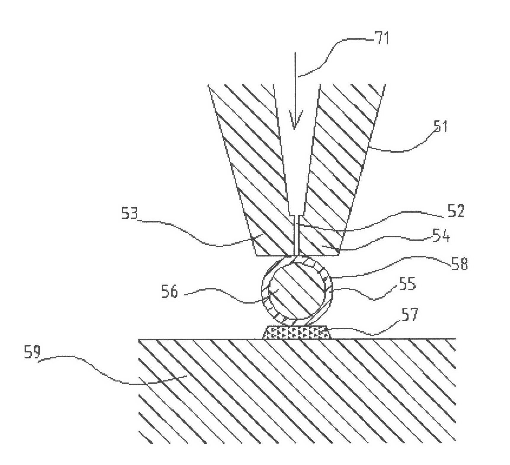
[0025] The structure adopts a metal antenna in the form of a copper coil and a high-frequency chip, so that the electronic label is packaged and processed by the present invention.

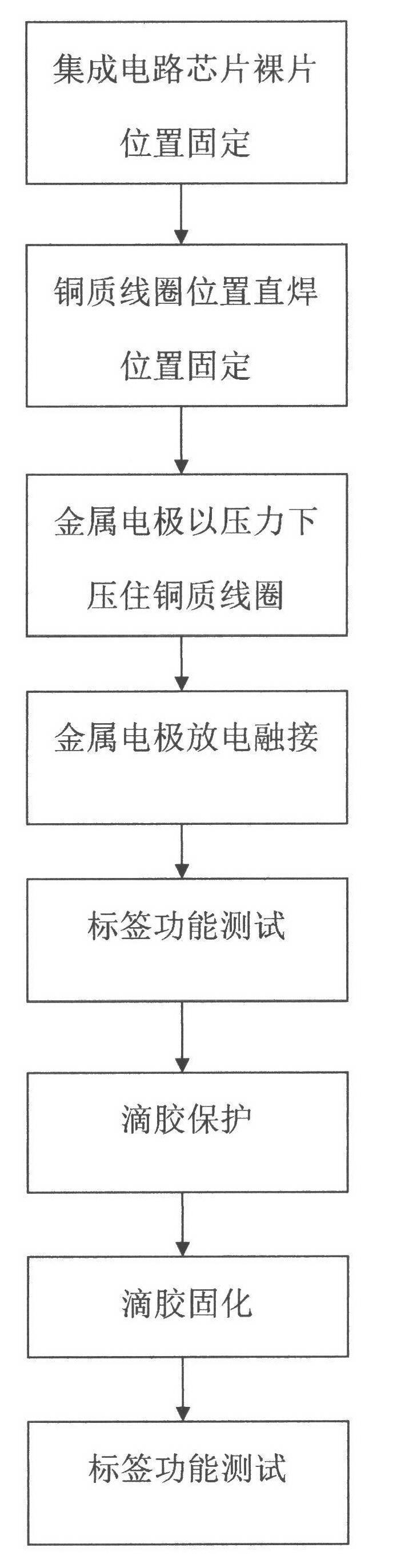
[0026] figure 1 It is a process flowchart of the present invention.

[0027] Firstly, the position of the integrated circuit chip die 59 is fixed.

[0028] The soldering position of the metal antenna (copper coil) 58 is just placed directly above the protruding external terminal 57 on the IC chip die 59 .

[0029] The metal electrode 51 presses the welding position of the metal antenna (copper coil) 58 with a certain pressure, so that the welding position of the metal antenna (copper coil) 58 is in contact with the protruding external terminal 57 on the IC chip die 59 .

[0030] The metal electrode 51 is discharged, and the metal antenna 58 is fused with the protruding external terminal 57 on the IC chip die 59 .

[0031] Perform a label functional test to confirm successful fusion.

[0032] A...


PUM


Abstract

The invention provides a direct welding processing method of an electronic label, which comprises a metal electrode 51, an integrated circuit chip bare chip 59, a protruding outer wiring terminal 57 arranged on the integrated circuit chip bare chip 59, a metal antenna 58 and dripping glue 62 for protection. The metal antenna 58 is placed above the protruding outer wiring terminal 57 arranged on the chip bare chip, and the metal electrode 51 with a bottom area divided into two poles 53 and 54 is adopted to exert a certain downward pressure on the metal antenna 58. When a certain instant voltage is loaded on the two poles 53 and 54 of the electrode, the two poles 53 and 54 of the electrode generate momentary discharge, the discharge causes a metal material 56 in an area contacted with the metal electrode to melt, soften in a short time and be in melting connection with the protruding outer wiring terminal 57 which is arranged on the chip and contacted with the bottom of the metal material, thereby achieving conducting connection between the metal antenna 58 and the integrated circuit chip bare chip 59. The dripping glue 62 for protection is adopted to protect all relevant portions combined with direct welding and the peripheries of the relevant portions, and solidification processing needs to be performed to the dripping glue.

Description

technical field [0001] The present invention relates to RFID (Radio Frequency Identification) electronic tags, in particular to a direct welding processing method for electronic tags. The electronic tags processed by this method have small package size of chips and high resistance to bending and impact. capabilities and advantages. Background technique [0002] In the chip packaging processing of electronic tags, Flip Chip (inverted packaging) process, COB (chip packaged on hard board) process, COF (chip packaged on soft board) and SOP (standard chip package) are commonly used. ) process. Using flip-top packaging technology and COB and COF packaging technology, the packaged chip cannot resist multiple high-strength bending, nor can it resist external force impact. It is packaged by SOP technology, which can withstand external impact, but it needs to use SMT (surface mount technology) for chip mounting, and the total processing cost of the electronic label is relatively hig...

Claims


Application Information

Patent Timeline
Patent Type & Authority Applications(China)
IPC IPC(8): H01L21/60G06K19/077
CPCH01L24/85H01L2224/05553H01L2224/4847H01L2224/85H01L2224/8592H01L2924/14H01L2924/00H01L2924/00012
Inventor 孙向荣
Owner 江苏安智博电子科技有限公司
Why Eureka
Eureka Blog
Learn More