Semiconductor field effect structure and preparation method and application thereof

A field effect, semiconductor technology, applied in the field of semiconductor field effect structure, to achieve the effect of a significant magnetic field

Active Publication Date: 2012-07-04
INST OF PHYSICS - CHINESE ACAD OF SCI
View PDF4 Cites 8 Cited by
  • Summary
  • Abstract
  • Description
  • Claims
  • Application Information

AI Technical Summary

Benefits of technology

This patented technology describes an improved way for creation of electronic device structures that are able to control their electrical behavior based upon external stimuli like light or pressure waves. These structures consist mainly made up of layers containing materials called Pervoskites (PM) and Ferroelectrics (F). By adding specific types of atoms into these components during manufacturing process they become magnetizable when exposed to certain conditions such as heat or mechanical stress. When this happens, there will be no net voltage across any electrodes within them due to the presence of electrons in one atom's position. Additionally, if another electron tries to enter at some point along the pathway between two points where charges move freely, then it causes a slight increase in current flow through nearby parts. Overall, this design allows for more precise controllability over how well things work without being affected by outside factors like temperature or power supply levels.

Problems solved by technology

This patents describes different types of materials called perovelceramics or perovscreens made up from these compounds. These materials display unique features like high electrostatic inductance, low coercion force, ferromagnetism, quantum interference effects, and reversible polarization caused by changes in ion concentration within specific sites along certain directions. They may find use in fields related to sensing/communicating systems, memory elements, transistor technology, and other technical problem addressed in this patented paper.

Method used


Image

  • Semiconductor field effect structure and preparation method and application thereof
  • Semiconductor field effect structure and preparation method and application thereof
  • Semiconductor field effect structure and preparation method and application thereof

Examples


Embodiment

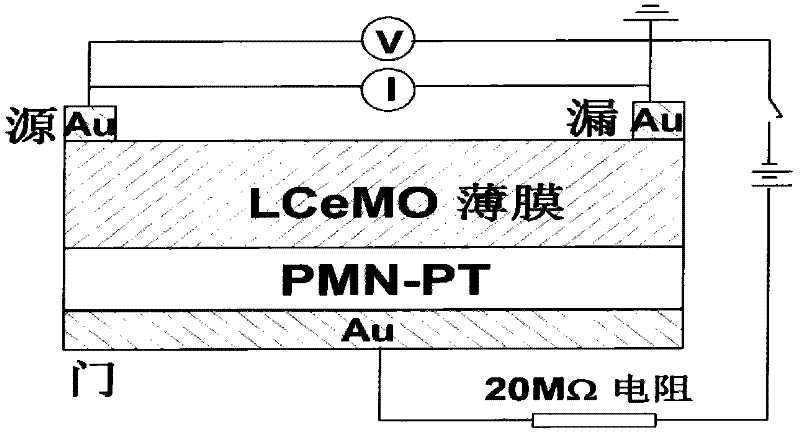
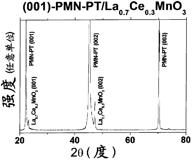
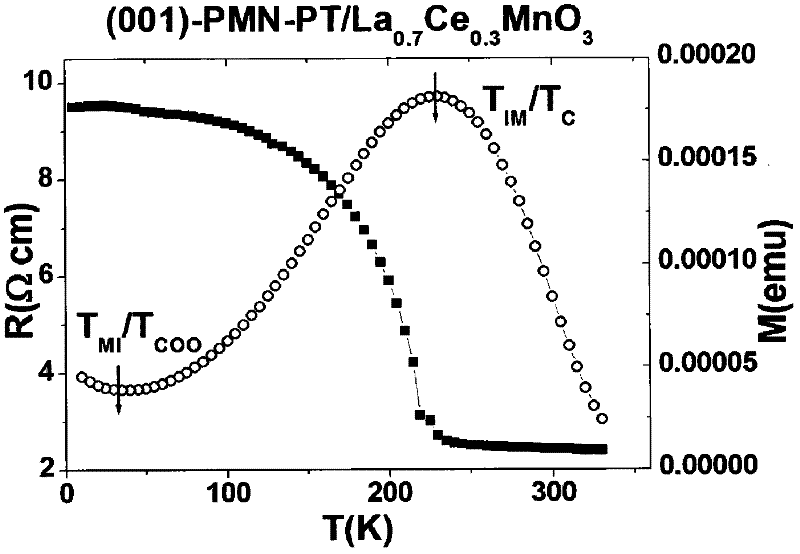
[0054] Embodiment (001)-0.7Pb(Mg 1 / 3 Nb 2 / 3 )O 3 -0.3PbTiO 3 (PMN-PT) / La 0.7 Ce 0.3 MnO 3 Fabrication of Field Effect Structures

[0055] La prepared by chemical formula 0.7 Ce 0.3 MnO 3 Perovskite manganese oxide, the specific steps are as follows:

[0056] 1) Press La 0.7 Ce 0.3 MnO 3 Chemical formula ingredient, raw material is La 2 o 3 , CeO 2 , MnCO 3 (MnCO 3 Decomposes during calcination, C forms CO 2 followed by airflow). After the proportioned raw materials are fully ground and mixed, they are calcined at 900 degrees Celsius for 24 hours. After taking it out, it was ground and calcined three times under the same conditions, and then sintered at 1300 degrees Celsius for 48 hours to prepare a La with a diameter of 40 mm and a thickness of 5 mm. 0.7 Ce 0.3 MnO 3 target.

[0057] 2) Purchase (001)-oriented 0.7Pb (Mg 1 / 3 Nb 2 / 3 )O 3 -0.3PbTiO 3 (PMN-PT) single crystal substrate (thickness 0.1mm). Before deposition, the PMN-PT substrate was ultras...


PUM


Abstract

The invention discloses a semiconductor field effect structure and a preparation method and application thereof. In the semiconductor field effect structure, a relaxation ferroelectric single-crystal substrate PMN-PT is used as a grid electrode and quadrivalent cation doped perovskite manganese oxide formed on the single-crystal substrate is used as a channel. Due to the relaxation ferroelectric single-crystal substrate PMN-PT having evident inverse piezoelectric effect, the channel resistance generated on the relaxation ferroelectric single-crystal substrate PMN-PT can be changed evidently by combination action of polarization induced by an electric field and strain effect, and accordingly a novel functional field effect structure having evident magnetic field and adjustable electric-field property is obtained. Meanwhile, the quadrivalent cation doped perovskite manganese oxide has n-type conductive property and the energy band structure is different from the P type, so that the field effect structure utilizing the quadrivalent cation doped perovskite manganese oxide as the channel has brand-new advantages of field effect.

Description


Claims


Application Information

Patent Timeline
Owner INST OF PHYSICS - CHINESE ACAD OF SCI
Why Eureka
Try Eureka