Semiconductor heterostructure, preparation method thereof and semiconductor device

A heterostructure and semiconductor technology, which is applied in the fields of semiconductor/solid-state device manufacturing, semiconductor devices, electrical components, etc., can solve the problems of complex preparation process and affect the functional characteristics of semiconductor heterostructures, and achieve simple preparation process and good rectification characteristics. , to eliminate the effect of interfacial diffusion

Inactive Publication Date: 2012-06-13
INST OF PHYSICS - CHINESE ACAD OF SCI
View PDF0 Cites 0 Cited by
  • Summary
  • Abstract
  • Description
  • Claims
  • Application Information

AI Technical Summary

Problems solved by technology

However, the interface barrier layer SrTiO 3 The emergence of not only complicates the preparation process, but also affects the functional properties of semiconductor heterostructures

Method used


Image

  • Semiconductor heterostructure, preparation method thereof and semiconductor device
  • Semiconductor heterostructure, preparation method thereof and semiconductor device
  • Semiconductor heterostructure, preparation method thereof and semiconductor device

Examples


Embodiment 1

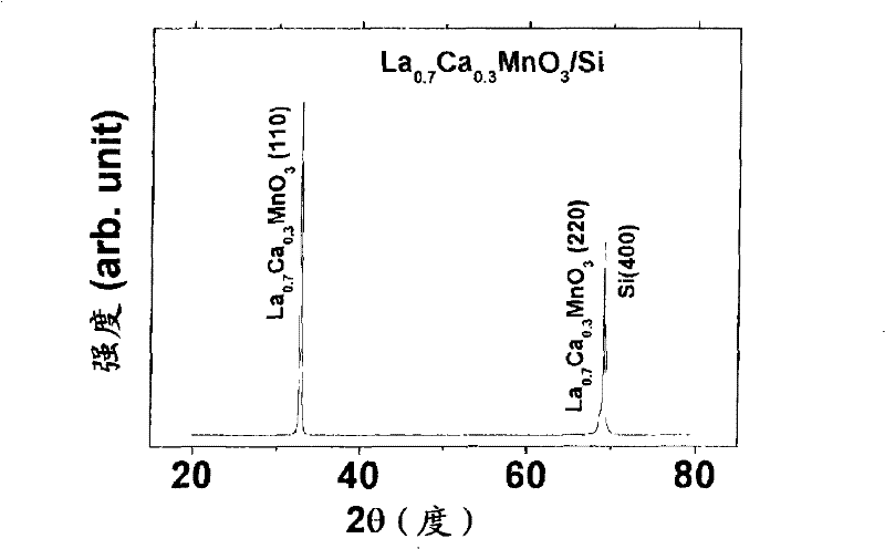
[0050] Example 1 Si / La 0.7 Ca 0.3 MnO 3 Fabrication of semiconductor heterostructures

[0051] La prepared by chemical formula 0.7 Ca 0.3 MnO 3 Perovskite manganese oxide, the specific process is:

[0052] 1) Press La 0.7 Ca 0.3 MnO 3 Chemical formula ingredient, raw material is La 2 o 3 , CaCO 3 , MnCO 3 (CaCO 3 , MnCO 3 Decomposes during calcination, C forms CO 2 followed by airflow). After the proportioned raw materials are fully ground and mixed, they are calcined at 900 degrees Celsius for 24 hours. After taking it out, it was ground and calcined three times under the same conditions, and then sintered at 1350 degrees Celsius for 48 hours to prepare a La with a diameter of 40 mm and a thickness of 5 mm. 0.7 Ca 0.3 MnO 3 target.

[0053] 2) Phosphorus-doped n-type single crystal silicon with a resistivity of 6Ω·cm is selected as the substrate, and the single crystal orientation is (100). Before deposition, the silicon substrate is first c...

Embodiment 2

[0059] Example 2 Si / La 0.7 Ba 0.3 MnO 3 Fabrication of semiconductor heterostructures

[0060] La prepared by chemical formula 0.7 Ba 0.3 MnO 3 Perovskite manganese oxide, the specific process is:

[0061] 1) Press La 0.7 Ba 0.3 MnO 3 The chemical formula ingredients, the raw material is La 2 o 3 , BaCO 3 , MnCO 3 (BaCO 3 , MnCO 3 Decomposes during calcination, C forms CO 2 followed by airflow). After fully grinding and mixing the raw materials prepared according to the proportion, calcining at 900 degrees Celsius for 24 hours. After taking it out, it was ground and calcined under the same conditions, repeated three times, and then sintered at 1350 degrees Celsius for 48 hours to prepare a La with a diameter of 40 mm and a thickness of 5 mm. 0.7 Ba 0.3 MnO 3 target.

[0062] 2) Phosphorus-doped n-type single crystal silicon with a resistivity of 6Ω·cm is selected as the substrate, and the single crystal orientation is (100). Before deposition...


PUM

PropertyMeasurementUnit
thicknessaaaaaaaaaa
electrical resistivityaaaaaaaaaa

Abstract

The invention discloses a semiconductor heterostructure which has no other introduced intercalations and is at least provided with a monocrystalline silicon substrate and a perovskite manganite formed on the monocrystalline silicon substrate. The invention also discloses a preparation method of the semiconductor heterostructure and a semiconductor device containing the semiconductor heterostructure. A perovskite manganite film directly grows on the silicon surface, and other matters are not introduced as a buffering layer in the growth process, therefore, not only the preparation process becomes simple, but also the problems and the defects of interfacial diffusion caused by the introduction of intermediate intercalations are eliminated. In the invention, the n-Si / p-R1-xAxMnO3 + / - Delta functional heterostructure with favorable rectifying property is obtained.

Description

technical field [0001] The invention relates to a semiconductor heterostructure composed of single crystal silicon and perovskite manganese oxide, its preparation method and semiconductor device. Background technique [0002] Perovskite manganese oxide has become a research hotspot in the world in recent years due to its colossal magnetoresistance (CMR) effect. More and more facts show that the potential advantage of perovskite manganese oxide lies in the preparation of magnetoelectronic devices. In addition to the extraordinary magnetoresistance effect, perovskite oxides also exhibit rich physical properties such as giant electric field resistance, ferroelectricity, dielectricity, and superconductivity, so they can be expected to be used to obtain practical devices with various novel functions. In fact, shortly after the discovery of the CMR effect, people tried to use perovskite manganese oxides to prepare magnetic tunnel junctions. As early as 1996, Lu et al. observed in...

Claims


Application Information

Patent Timeline
Patent Type & Authority Patents(China)
IPC IPC(8): H01L29/06H01L21/20C04B35/622
Inventor 胡凤霞王晶孙继荣沈保根
Owner INST OF PHYSICS - CHINESE ACAD OF SCI
Why Eureka
Try Eureka