A photodiode device and a method for producing a rectification effect

A photodiode and electrode technology, applied in circuits, electrical components, semiconductor devices, etc., can solve the problems of no improvement in photoelectric response speed, vertical structure restrictions on application, etc., and achieve high photoelectric conversion efficiency and obvious rectification characteristics.

Active Publication Date: 2018-03-02
INST OF PHYSICS - CHINESE ACAD OF SCI
View PDF12 Cites 0 Cited by
  • Summary
  • Abstract
  • Description
  • Claims
  • Application Information

AI Technical Summary

Problems solved by technology

Due to the limitation of the mobility of carriers in semiconductor materials, the photoelectric response speed of this graphene / semiconductor Schottky junction photodiode is not improved compared with commercial silicon-based photodiodes, and is still on the order of microseconds; in addition , its vertical structure limits its application in planar integration and micro-nano devices

Method used


Image

  • A photodiode device and a method for producing a rectification effect
  • A photodiode device and a method for producing a rectification effect
  • A photodiode device and a method for producing a rectification effect

Examples


Embodiment Construction

[0027] In order to make the object, technical solution and advantages of the present invention clearer, the present invention will be further described in detail below through specific embodiments in conjunction with the accompanying drawings. It should be understood that the specific embodiments described here are only used to explain the present invention, not to limit the present invention.

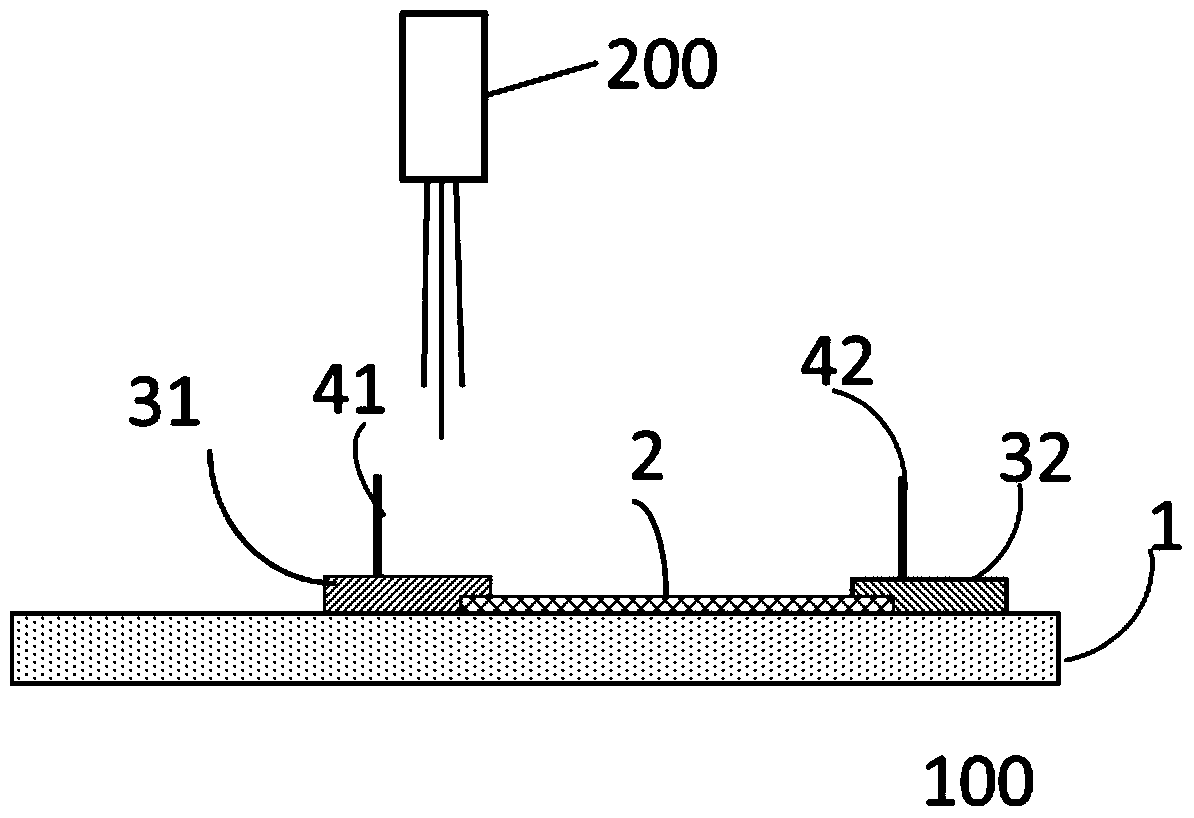
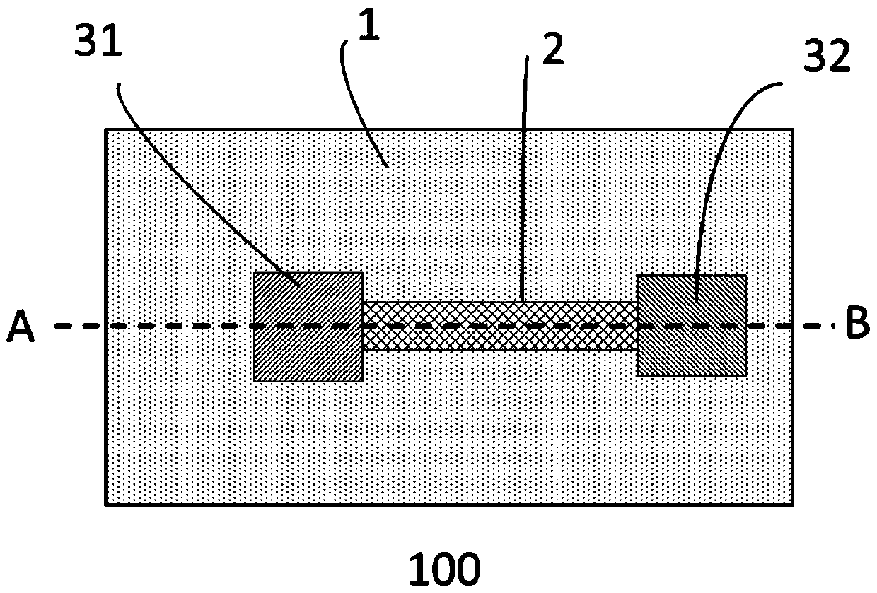
[0028] In order to fully utilize and excavate the role of all participating components in the photodiode device based on ITO and graphene, the present invention proposes a photodiode device whose substrate is absorbable to irradiated light. Since the thickness of the substrate material is much larger than that of the ITO electrode or graphene, the photogenerated carriers generated by its efficient absorption of irradiated light can be absorbed by the substrate / ITO interface electric field and the substrate / graphene interface electric field. Rapid transfer into ITO electrodes or graphen...


PUM


Abstract

The invention relates to a photodiode device. The photodiode device comprises a light source and a rectifying structure; the rectifying structure comprises a high-resistance light gain semiconductor substrate, a graphene layer located on the high-resistance light gain semiconductor substrate, a first ITO electrode and a second electrode, wherein the first ITO electrode and the second electrode are located on the high-resistance light gain semiconductor substrate and the graphene layer, one part of the first ITO electrode and one part of the second electrode contact with the high-resistance light gain semiconductor substrate, and the other part of the first ITO electrode and the other part of the second electrode contact with the graphene layer; the energy of light emitted by the light source is greater than the band gap of the high-resistance light gain semiconductor substrate, and the light source only irradiates the first ITO electrode; and the area of the ITO electrode is larger than the area of the light spot of the light emitted by the light source. The photodiode device of the invention is of a planar structure and has high photoelectric response speed and can be potentially applied to the planar integration and micro-nano device field.

Description

technical field [0001] The invention belongs to the technical field of semiconductors, and in particular relates to a photodiode device and a method for generating a rectification effect. Background technique [0002] Graphene is a new type of two-dimensional material composed of honeycomb-shaped carbon atoms, which has a unique linear energy band structure, excellent electrical properties, large specific surface area, mechanical strength and good chemical stability. There have been a large number of reports on the combination of graphene and traditional semiconductors (especially semiconductor silicon materials) to prepare Schottky junction devices [see arXiv: 1505.07686 (2015)]. As the main structural unit of modern semiconductor devices, Schottky junction has been widely used in modern semiconductor optoelectronic components and systems. Existing solar cells and photodiodes based on graphene / semiconductor Schottky junctions have all adopted graphene / semiconductor (doped)...

Claims


Application Information

Patent Timeline
Patent Type & Authority Patents(China)
IPC IPC(8): H01L31/101H01L31/102H01L31/0224
CPCH01L31/0224H01L31/022408H01L31/101H01L31/102
Inventor 郭丽伟陈小龙黄郊史哲
Owner INST OF PHYSICS - CHINESE ACAD OF SCI
Why Eureka
Try Eureka