Semiconductor field effect structure and preparation method and application thereof
A field effect, semiconductor technology, applied in the field of semiconductor field effect structure, to achieve the effect of a significant magnetic field
- Summary
- Abstract
- Description
- Claims
- Application Information
AI Technical Summary
Problems solved by technology
Method used
Image
Examples
Embodiment
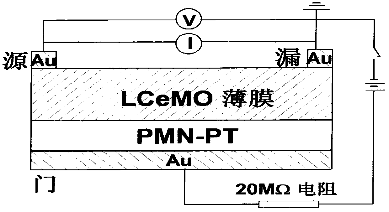
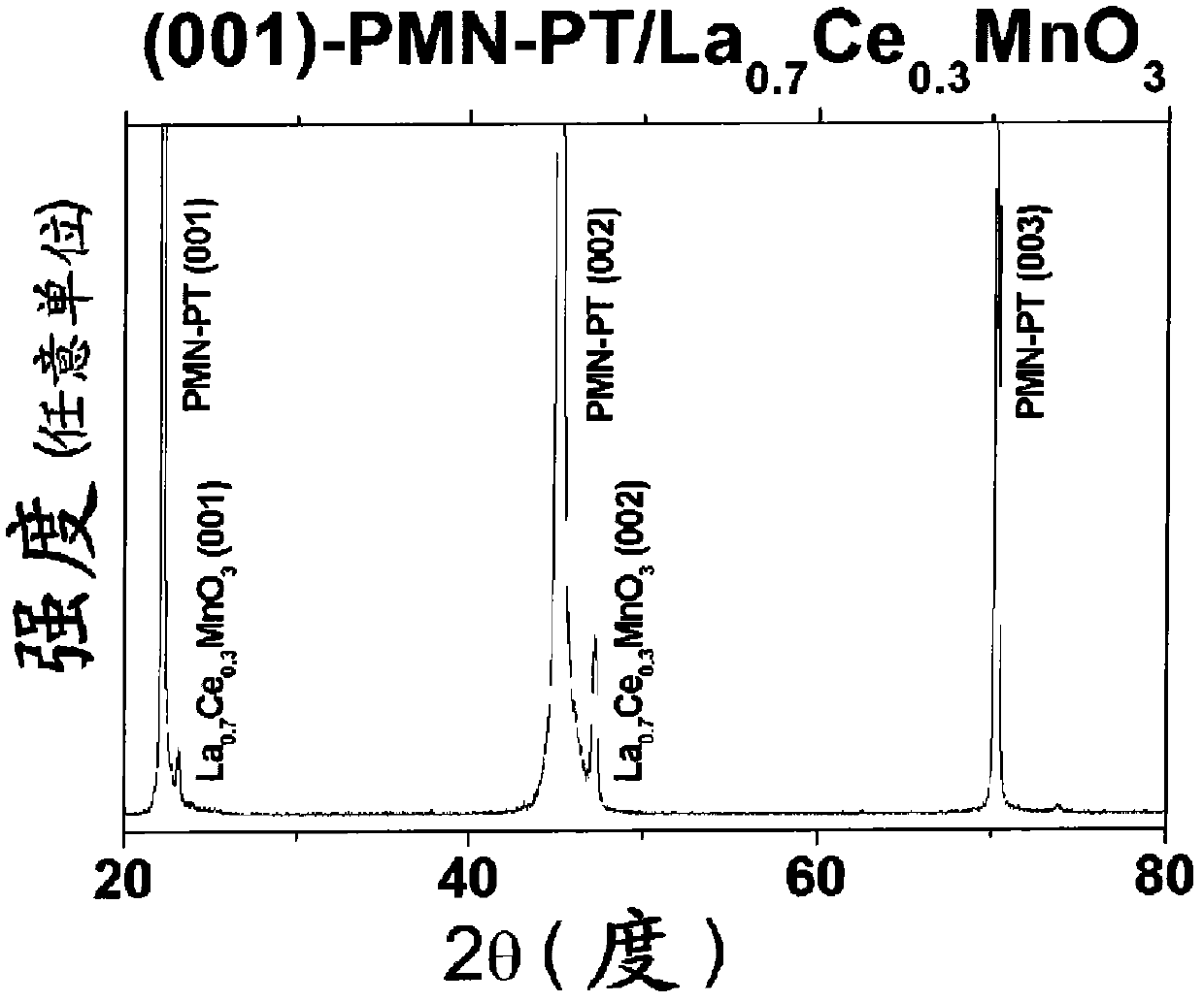
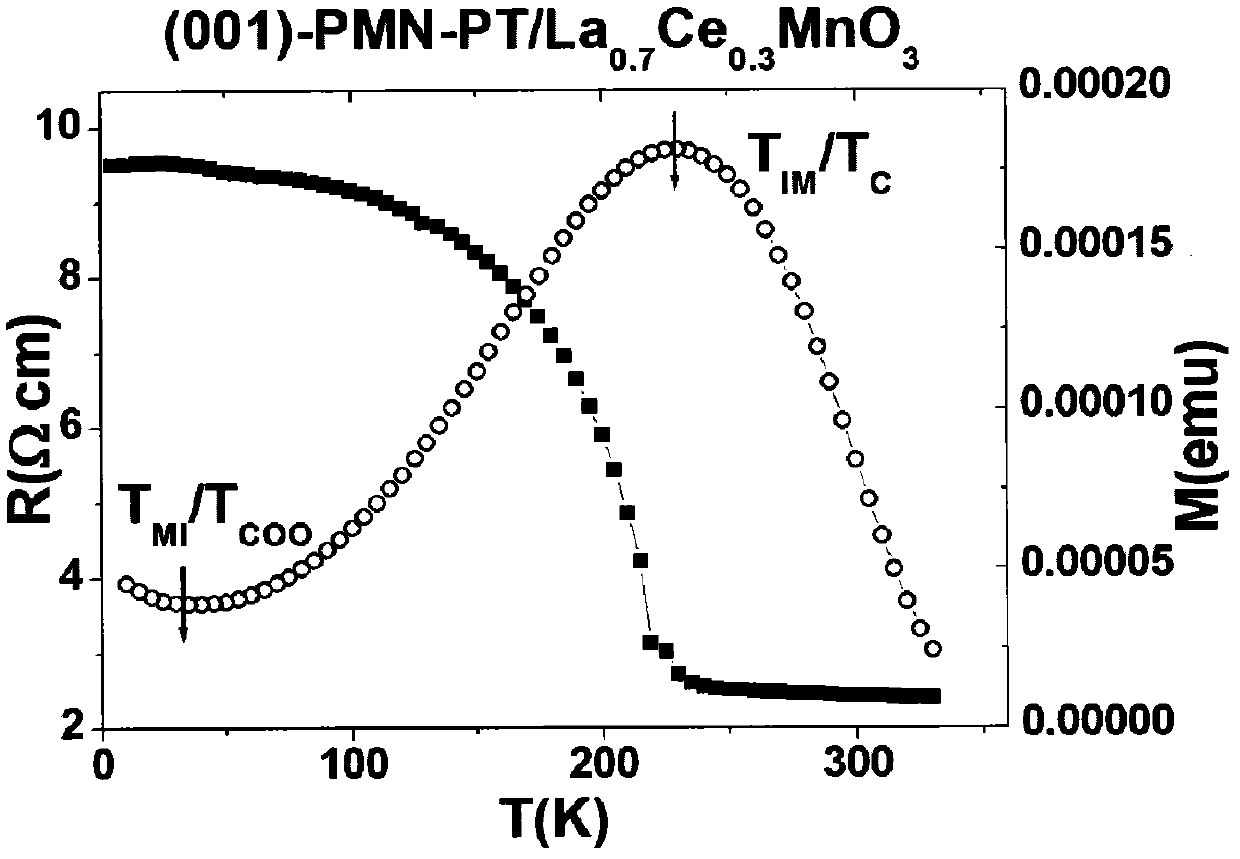
[0054] Embodiment (001)-0.7Pb(Mg 1 / 3 Nb 2 / 3 )O 3 -0.3PbTiO 3 (PMN-PT) / La 0.7 Ce 0.3 MnO 3 Fabrication of Field Effect Structures
[0055] La prepared by chemical formula 0.7 Ce 0.3 MnO 3 Perovskite manganese oxide, the specific steps are as follows:
[0056] 1) Press La 0.7 Ce 0.3 MnO 3 Chemical formula ingredient, raw material is La 2 o 3 , CeO 2 , MnCO 3 (MnCO 3 Decomposes during calcination, C forms CO 2 followed by airflow). After the proportioned raw materials are fully ground and mixed, they are calcined at 900 degrees Celsius for 24 hours. After taking it out, it was ground and calcined three times under the same conditions, and then sintered at 1300 degrees Celsius for 48 hours to prepare a La with a diameter of 40 mm and a thickness of 5 mm. 0.7 Ce 0.3 MnO 3 target.
[0057] 2) Purchase (001)-oriented 0.7Pb (Mg 1 / 3 Nb 2 / 3 )O 3 -0.3PbTiO 3 (PMN-PT) single crystal substrate (thickness 0.1mm). Before deposition, the PMN-PT substrate was ultras...
PUM
| Property | Measurement | Unit |
|---|---|---|
| thickness | aaaaa | aaaaa |
| thickness | aaaaa | aaaaa |
| thickness | aaaaa | aaaaa |
Abstract
Description
Claims
Application Information


