Oxide semiconductor heterostructure modulated by biasing electric field, preparing method and device thereof
A technology of oxide semiconductors and heterostructures, which is applied in semiconductor/solid-state device manufacturing, semiconductor devices, circuits, etc., can solve the problems of limiting practical applications, rectification behavior does not have electric field adjustment characteristics, etc.
- Summary
- Abstract
- Description
- Claims
- Application Information
AI Technical Summary
Problems solved by technology
Method used
Image
Examples
Embodiment
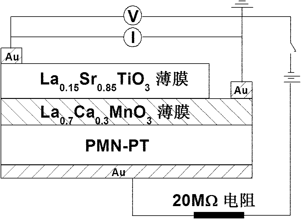
[0075] Example: All-Oxide Heterostructures Grown on PMN-PT Substrates (001)-0.7Pb(Mg 1 / 3 Nb 2 / 3 )O 3 -0.3PbTiO 3 (PMN-PT) / p-La 0.7 Ca 0.3 MnO 3 / n-La 0.15 Sr 0.85 TiO 3 preparation of
[0076] 1) Preparation of hole-type perovskite manganese oxide p-La 0.7 Ca 0.3 MnO 3 Target:
[0077] Press La 0.7 Ca 0.3 MnO 3 Chemical formula ingredient, raw material is La 2 o 3 (purity: 99.99%), CaCO 3 (purity: 99.9%), MnCO 3 (Purity: 99.9%); After grinding and mixing the raw materials thoroughly, calcining at 900 degrees Celsius for 12 hours, taking out and grinding again, calcining again under the same conditions, repeating 3-4 times, and finally sintering at 1300 degrees Celsius to form La 0.7 Ca 0.3 MnO 3 target;
[0078] 2) Preparation of electronic perovskite oxide n-La 0.15 Sr 0.85 TiO 3 Target:
[0079] Press La 0.15 Sr 0.85 TiO 3 Chemical formula ingredient, raw material is La 2 o 3 (purity: 99.99%), SrCO 3 (...
PUM
 Abstract
Description
Claims
Application Information


