Pattern matching method, pattern matching program, electronic computer, and electronic device testing apparatus
A matching method and technology of electronic equipment, applied in computing, measuring device, image enhancement and other directions, can solve problems such as difficulty in setting search benchmarks, difficulty in searching checkpoints, etc., and achieve the effect of simplifying setting operations
- Summary
- Abstract
- Description
- Claims
- Application Information
AI Technical Summary
Problems solved by technology
Method used
Image


Examples
Embodiment approach 1
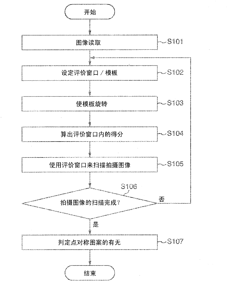
[0039] figure 1 It is a flowchart illustrating the procedure of the pattern matching method according to Embodiment 1 of the present invention.
[0040] figure 1 The procedure shown in the flow chart of the figure shows a method of pattern matching used in which an electronic device is photographed by an imaging device such as an optical microscope, and an inspection point is inspected using the photographed image. In this process, the above-mentioned photographed image can be received and executed by a computer or the like that executes the same procedure. The same applies to the following embodiments.
[0041] The term "electronic equipment" here refers to devices such as semiconductor devices to be inspected.
[0042] This electronic computer includes an arithmetic unit, a captured image input unit, an image display unit, and an operation input unit.
[0043] The computing device is composed of a CPU (Central Processing Unit) or a microcomputer, etc., and executes figu...
Embodiment approach 2
[0097] In Embodiment 2 of the present invention, a method for improving the effect of pattern matching will be described excluding elements that adversely affect the matching score of pattern matching. In addition, the method described in Embodiment 2 may be used in combination with the method described in Embodiment 1 or may be performed independently.
[0098] As an example of a captured image including elements that adversely affect the matching score of pattern matching, the figure 2 captured image. In this image, besides the scribed line 203, there is also a rectangular pattern.
[0099] Such patterns other than dashed lines affect the matching score when searching for point-symmetrical patterns by pattern matching, so it is preferable to remove them if possible.
[0100] Hereinafter, a method of searching for a point-symmetrical pattern after removing such a pattern that affects the matching score from the captured image will be described.
[0101] In addition, in th...
Embodiment approach 3
[0141] In Embodiment 3 of the present invention, a pattern matching method in which a reference image to be used for pattern matching can be selected by an inspector or the like will be described. In addition, conditions for optimizing pattern matching in accordance with the selected reference image will be described.
[0142] In addition, in the third embodiment, an effort is made to make the examiner who is used to the conventional pattern matching method unaware of the difference in the pattern matching method. Specifically, when the computing device reports the pattern matching result, it executes a process of correcting the report format in accordance with the existing pattern matching method. Details will be described later.
[0143] Figure 10 It is a flowchart illustrating the procedure of the pattern matching method according to the third embodiment. Figure 10 The procedures shown in the flow charts of FIG. Below, explain Figure 10 each step.
[0144] ( Figu...
PUM
 Abstract
Description
Claims
Application Information
 - R&D
- Intellectual Property
- Life Sciences
- Materials
- Tech Scout
- Unparalleled Data Quality
- Higher Quality Content
- 60% Fewer Hallucinations
Browse by: Latest US Patents, China's latest patents, Technical Efficacy Thesaurus, Application Domain, Technology Topic, Popular Technical Reports.
© 2025 PatSnap. All rights reserved.Legal|Privacy policy|Modern Slavery Act Transparency Statement|Sitemap|About US| Contact US: help@patsnap.com