High-power electronic ballast
An electronic ballast and high-power technology, applied in the field of high-power electronic ballasts, can solve the problems of damaging MOSFET tubes and shortening the service life of electronic ballasts.
- Summary
- Abstract
- Description
- Claims
- Application Information
AI Technical Summary
Problems solved by technology
Method used
Image
Examples
Embodiment Construction
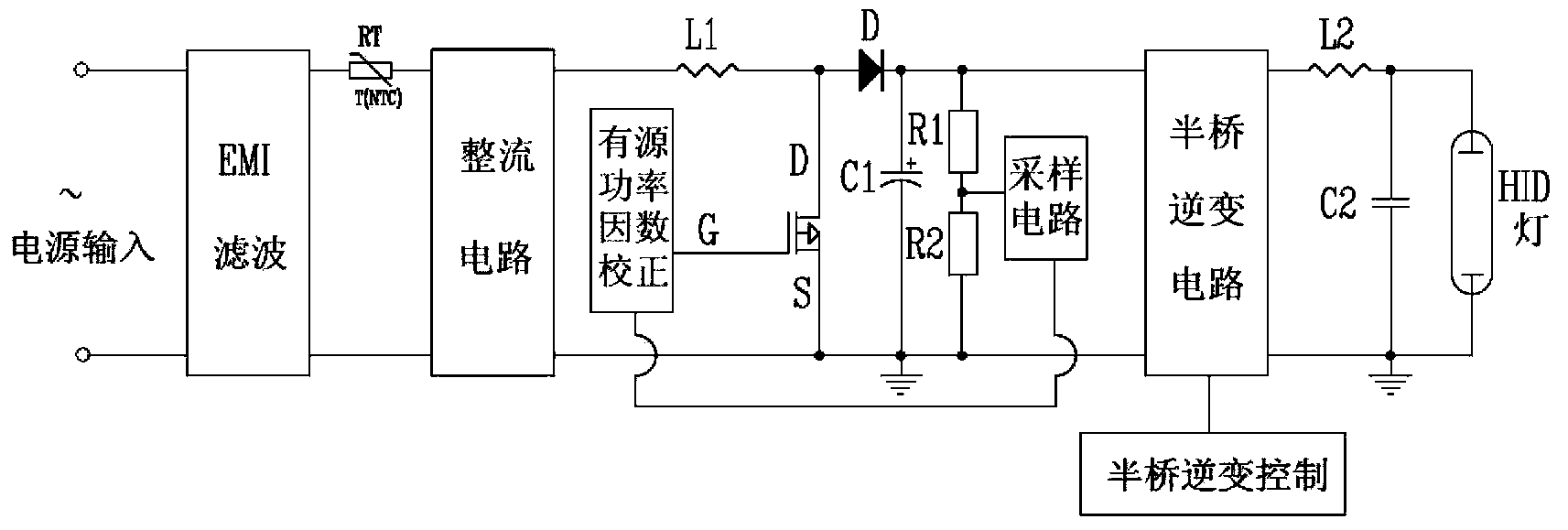
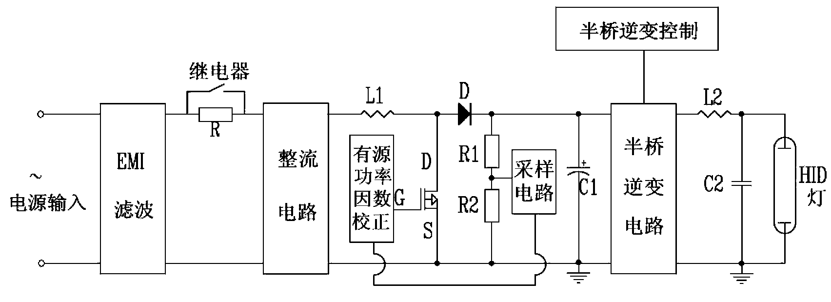
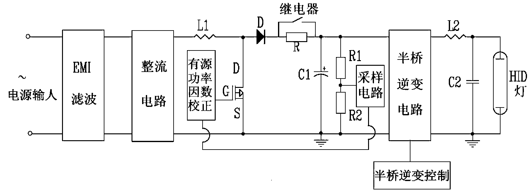
[0012] A high-power electronic ballast, which includes an EMI filter circuit 10, a rectifier circuit 20, an MCU control circuit 50, a sampling detection circuit 40, a half-bridge inverter circuit 60, a first inductor L11, a second inductor L12, a diode D11, Field effect transistor QE, first resistor R11, second resistor R12, third resistor R13, relay K, first capacitor C11, second capacitor C12 and HID lamp, EMI filter circuit 10 and rectifier circuit 20 connected in series, rectifier circuit The output terminal of 20 is connected to one end of the first inductance L11, and the other end of the first inductance L11 is respectively connected to the drain D of the field effect transistor QE and the anode of the diode D11, and it is characterized in that: the gate G of the field effect transistor QE passes through The PFC boost circuit 30 is connected to the MCU control circuit 50, the cathode of the diode D11 is respectively connected to one end of the second resistor R12 and one...
PUM
 Abstract
Description
Claims
Application Information


