
Flash memory unit and floating gate forming method thereof

A technology of flash memory cells and floating gates, which is applied in the fields of electrical components, semiconductor/solid-state device manufacturing, semiconductor devices, etc. It can solve the problems of high process cost, poor data retention, and inability to form double-doped structure floating gates to achieve programming efficiency. High and strong data retention

Active Publication Date: 2012-09-26
SEMICON MFG INT (SHANGHAI) CORP
View PDF5 Cites 2 Cited by
  • Summary
  • Abstract
  • Description
  • Claims
  • Application Information

AI Technical Summary

Problems solved by technology

[0008] The present invention solves the problems that in the prior art, it is impossible to form a flash memory unit with a double-doped structure floating gate and a small critical size, and the existing flash memory unit has low programming efficiency, poor data retention, and high process cost.

Method used


Image

  • Flash memory unit and floating gate forming method thereof
  • Flash memory unit and floating gate forming method thereof
  • Flash memory unit and floating gate forming method thereof

Examples


Embodiment Construction

[0037] In order to make the above objects, features and advantages of the present invention more comprehensible, specific implementations of the present invention will be described in detail below in conjunction with the accompanying drawings.

[0038] In the following description, specific details are set forth in order to provide a thorough understanding of the present invention. However, the present invention can be implemented in many other ways than those described here, and those skilled in the art can make similar extensions without departing from the connotation of the present invention. Accordingly, the present invention is not limited to the specific embodiments disclosed below.

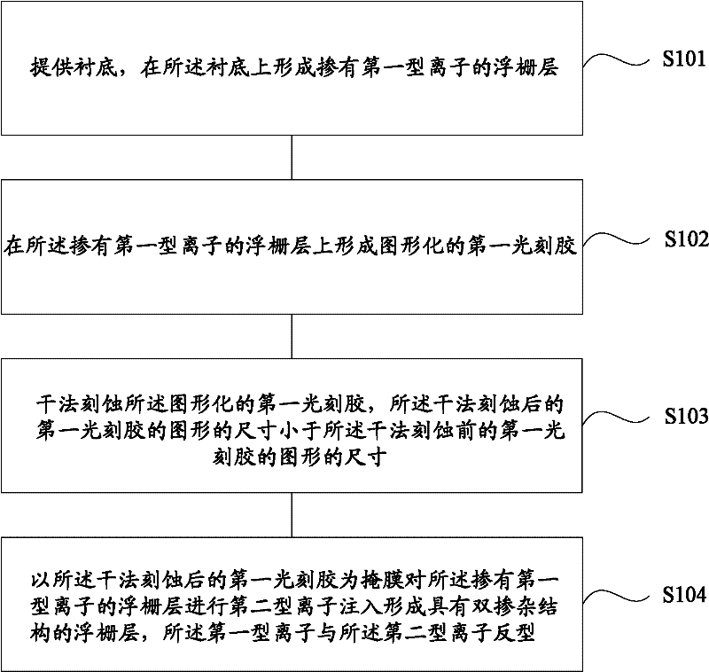
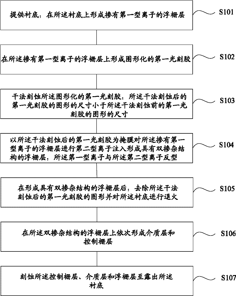
[0039] See figure 1 , figure 1 It is a flowchart of a method for forming a floating gate of a flash memory unit according to an embodiment of the present invention, including the following steps:

[0040] S101: providing a substrate, and forming a floating gate layer doped with first-typ...


PUM


Abstract

Provided are a flash memory unit and a floating gate forming method thereof. The floating gate forming method of the flash memory unit comprises the following steps of providing a substrate on which a floating gate layer doped with first type ions is formed; forming a graphical first photoresist on the floating gate layer doped with the first type ions; etching the graphical first photoresist through a dry method, wherein the figure of the first photoresist after etching through the dry method has a smaller dimension than the figure of the first photoresist before etching through the dry method; and performing a second type ion injection to the floating gate layer doped with the first type ions by using the first photoresist after etching through the dry method as a mask layer to form a floating gate layer with a double doped structure, wherein the first type ions is inversed with the second type ions. According to the floating gate of the flash memory unit and the flash memory unit forming method, the flash memory unit that is small in critical dimension and has the double doped floating gate structure can be produced, and the flash memory unit is high in programming efficiency, high in data maintenance capability and low in cost of processing.

Description

technical field [0001] The invention relates to the technical field of semiconductors, in particular to a flash memory unit and a method for forming a floating gate thereof. Background technique [0002] Generally speaking, semiconductor memory is divided into volatile memory and non-volatile memory. Volatile memory is prone to lose its data when power is turned off, and non-volatile memory can maintain on-chip information even after power supply is interrupted. [0003] Non-volatile memory includes electrically programmable read-only memory (EPROM), electrically erasable programmable read-only memory (EEPROM) and flash memory (flash memory). Compared with other non-volatile memories, flash memory has the characteristics of non-volatile data storage, low power consumption, high integration, fast access speed, easy erasing and rewriting, and low cost. Therefore, it is widely used in various fields. Such as: embedded systems, PCs and peripherals, telecommunications switches,...

Claims


Application Information

Patent Timeline
Patent Type & Authority Applications(China)
IPC IPC(8): H01L21/28H01L21/265H01L21/8247
CPCH01L29/7881H01L21/28123H01L29/66825H01L29/42324H01L21/28273H01L29/40114
Inventor 曾贤成李绍彬
Owner SEMICON MFG INT (SHANGHAI) CORP
Learn More