

Solid-state imaging device, method of manufacturing solid-state imaging device, and electronic device
A solid-state imaging device and electrode technology, which is applied in the direction of electric solid-state devices, radiation control devices, circuits, etc., can solve problems such as difficult design, and achieve the effect of increasing production and reducing changes
Active Publication Date: 2016-05-25
SONY CORP
View PDF5 Cites 0 Cited by
- Summary
- Abstract
- Description
- Claims
- Application Information
AI Technical Summary
Problems solved by technology
In such a structure, the transfer channel and the overflow channel are basically the same when transferring signal charges, so it is difficult to design
Method used
View moreImage
Smart ImageViewing Examples

Examples
no. 1 approach
[0034] 1. First Embodiment: Solid-state Imaging Device
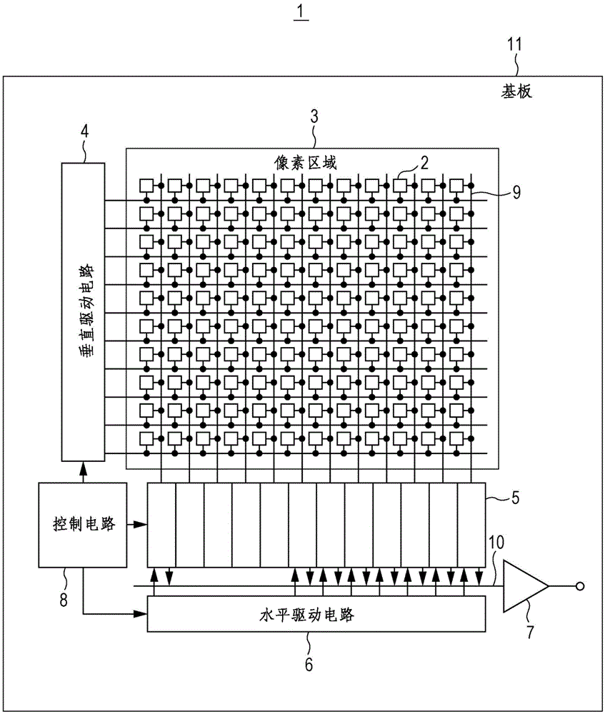
[0035] 1-1. Overall structure of solid-state imaging device
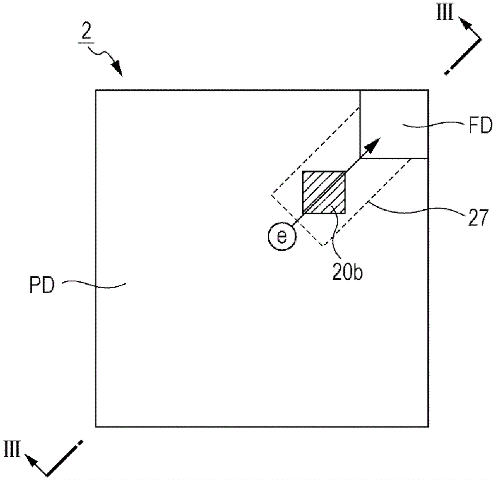
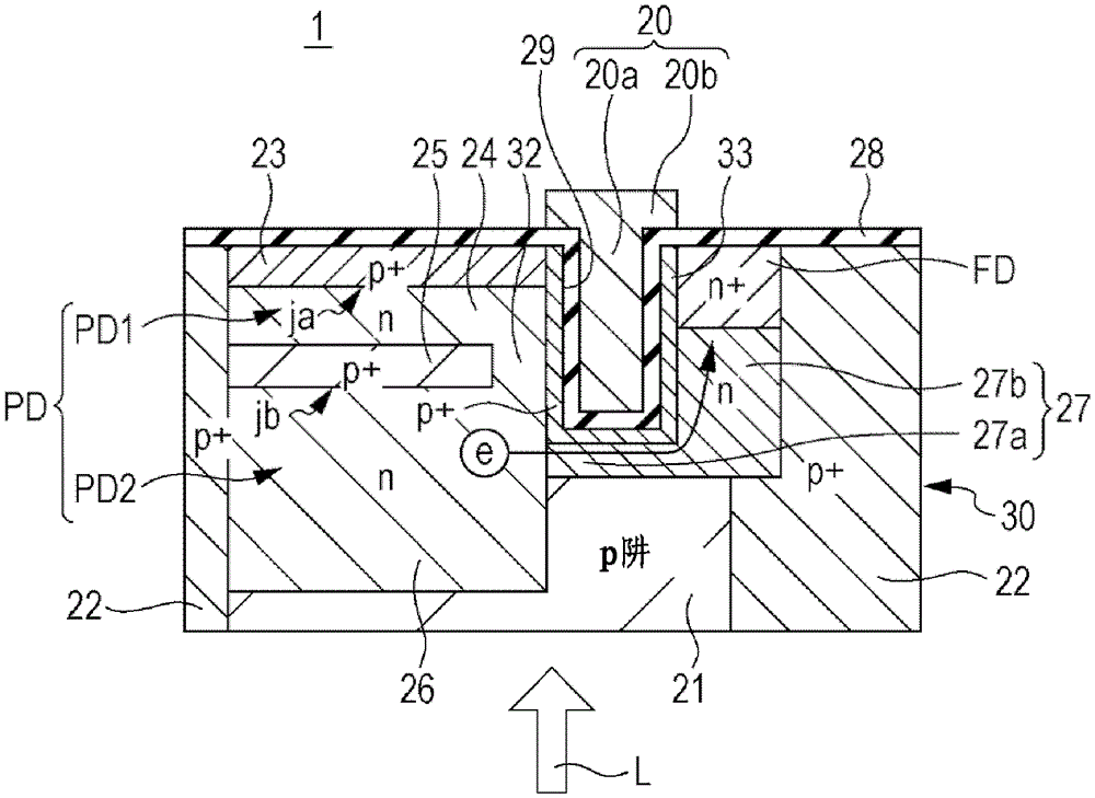
[0036] 1-2. Structure of main parts
[0037] 1-3. Manufacturing method
[0038] 1-4. Operation
[0039] 1-5. Modification 1
[0040] 1-6. Modification 2
no. 2 approach
[0041] 2. Second Embodiment: Manufacturing Method of Solid-State Imaging Device
no. 3 approach
[0042] 3. Third Embodiment: Manufacturing Method of Solid-State Imaging Device
Login to View More PUM
 Abstract
The invention discloses a solid-state imaging device, its manufacturing method and electronic equipment. The solid-state imaging device includes: a substrate; a photoelectric conversion unit formed on the substrate, the photoelectric conversion unit generating and accumulating signal charges according to a light quantity of incident light; a vertical transfer gate electrode, the A transfer gate electrode is formed to be embedded in a groove portion formed in a depth direction from one side surface of the substrate according to a depth of the photoelectric conversion unit; and an overflow channel, the An overflow channel that overflows signal charges accumulated in the photoelectric conversion unit is formed at the bottom of the transfer gate electrode. According to the present invention, in a solid-state imaging device provided with a vertical transfer transistor, variation in the amount of saturation charge is reduced, and yield is improved.
Description
[0001] Cross References to Related Applications [0002] This application contains subject matter related to that disclosed in Japanese Priority Patent Application JP2011-063974 filed in Japan Patent Office on Mar. 23, 2011, the entire content of which is hereby incorporated by reference. technical field [0003] The present invention relates to a solid-state imaging device having a vertical transistor, a method of manufacturing the solid-state imaging device, and electronic equipment provided with the solid-state imaging device. Background technique [0004] Solid-state imaging devices are classified into amplified solid-state imaging devices represented by devices such as complementary metal oxide semiconductor (Complementary Metal Oxide Semiconductor, CMOS) image sensors, or charge-coupled device (Charge Coupled Device, CCD) image sensors represented by devices such as charge coupled devices. Transmission type solid-state imaging device. Solid-state imaging devices are w...
Claims
Login to View More Application Information
Patent Timeline
 Patent Type & AuthorityPatents(China)
IPC IPC(8): H01L27/146
CPCH01L27/14607H01L27/1461H01L27/14612H01L27/14641H01L27/14656H01L27/14689H01L27/14643H01L27/14614H01L27/14625H01L27/1464
Inventor中村良助
OwnerSONY CORP