
Method for preparing double-faced back contact solar cell
A solar cell and back-contact technology, applied in the field of solar cells, can solve problems such as complex process, damage to the non-expanded boron suede surface, and complicated operation, and achieve the effects of simple preparation process, improved quality, and simplified process flow
- Summary
- Abstract
- Description
- Claims
- Application Information
AI Technical Summary
Problems solved by technology
Method used
Image

Examples
Embodiment 1
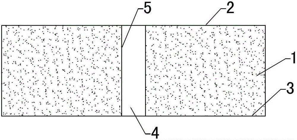
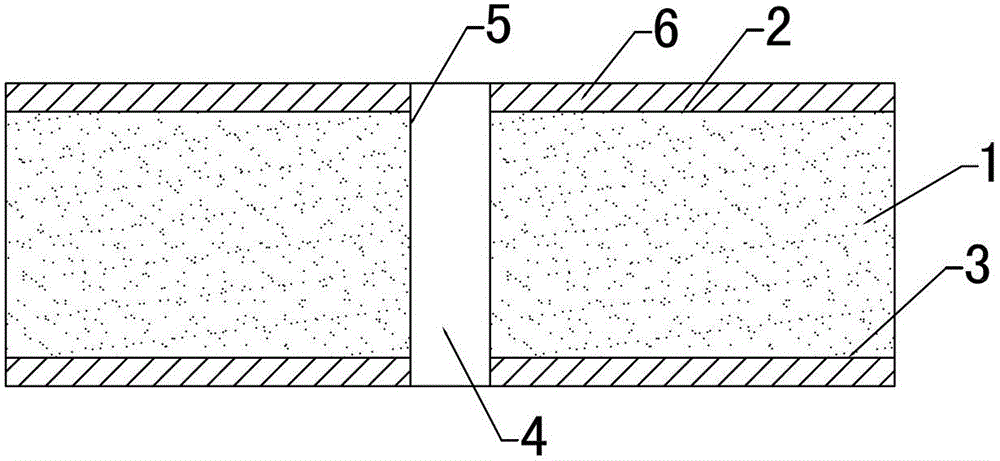
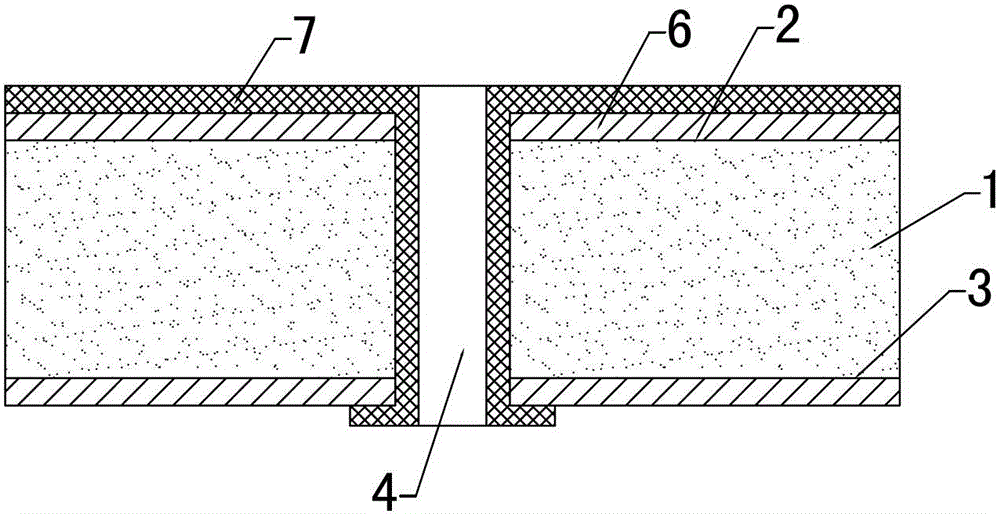
[0051] see Figure 1~9 Shown, a kind of preparation method of double-sided back-contact solar cell comprises the steps:
[0052] (1) Open a hole on the N-type silicon chip 1, and the hole wall 5 of the hole 4 is as figure 1 shown;
[0053] (2) Clean the surface of the silicon chip, remove the damaged layer, and carry out texturing on the front side 2 and the back side 3 of the silicon chip to form a textured surface 6, such as figure 2 shown;
[0054] (3) Print boron paste 7 on the front side of the silicon wafer and in the holes, the mass concentration of boric acid in the boron paste is 20%, and dry at 250°C for 2 minutes; print boron paste on the area around the hole on the back of the silicon wafer, and dry at 250°C 2 minutes, such as image 3 ;
[0055] (4) Phosphorus paste 8 is printed on the non-peripheral area of the backside of the silicon wafer, the mass concentration of phosphoric acid in the phosphorous paste is 25%, and it is dried at 250°C for 2 minutes, ...
Embodiment 2
[0063] see Figure 10~18 Shown, a kind of preparation method of double-sided back-contact solar cell comprises the steps:
[0064] (1) Clean the surface of the N-type silicon chip 1, remove the damaged layer, and make texture on the front side 2 and the back side 3 of the silicon chip to form a textured surface 6, such as Figure 10 ;
[0065] (2) Print boron paste 7 on the front side of the silicon wafer, the mass concentration of boric acid in the boron paste is 20%, and dry at 250°C for 2 minutes, as Figure 11 ;
[0066] (3) Phosphate paste 8 is printed on the non-hole area on the back of the silicon wafer, the mass concentration of phosphoric acid in the phosphor paste is 30%, and it is dried at 250°C for 2 minutes, as Figure 12 ;
[0067] (4) PECVD is used to deposit a silicon oxide barrier layer 9 on the front and back sides of the silicon wafer, and its thickness is 90nm, such as Figure 13 ;
[0068] (5) Anneal the silicon wafer obtained in step (4) at 900°C to...
Embodiment 3
[0074] A method for preparing a double-sided back-contact solar cell, comprising the steps of:
[0075] (1) Open holes on the P-type silicon wafer;
[0076] (2) Clean the surface of the silicon wafer, remove the damaged layer, and make texture on the front and back of the silicon wafer to form a textured surface;
[0077] (3) Print phosphorous slurry on the front side of the silicon wafer and in the holes, the mass concentration of phosphoric acid in the phosphorous slurry is 15%, and dry at 250°C for 2 minutes; print phosphorous paste on the area around the hole on the back of the silicon wafer, and dry at 250°C for 2 minute;
[0078] (4) Print boron paste on the non-peripheral area of the backside of the silicon wafer, the mass concentration of boric acid in the boron paste is 30%, and dry at 250°C for 2 minutes;
[0079] (5) PECVD is used to deposit a silicon oxide barrier layer on the front and back sides of the silicon wafer, with a thickness of 90nm;
[0080] (6) An...
PUM
 Abstract
Description
Claims
Application Information