Supercharge Your Innovation With Domain-Expert AI Agents!

Chemical mechanical polishing system and method of polishing wafer using the system

A technology of chemical machinery and wafers, which is applied in the direction of grinding devices, grinding machine tools, electrical components, etc., can solve the problems such as the inability to adjust the influence, and achieve the effect of avoiding changes in surface morphology, compensating for the reduction of grinding rate, and maintaining a constant effect

Active Publication Date: 2014-10-01
SEMICON MFG INT (SHANGHAI) CORP
View PDF3 Cites 0 Cited by
  • Summary
  • Abstract
  • Description
  • Claims
  • Application Information

AI Technical Summary

Problems solved by technology

That is to say, the existing chemical mechanical polishing process all adopts the same process parameters in the different stages of use of the grinding pad 110 and the finishing disc 152, therefore, it is impossible to adjust the prolongation of the service time due to the grinding pad 110 and the finishing disc 152. Influence of mechanical grinding process

Method used


Image

  • Chemical mechanical polishing system and method of polishing wafer using the system
  • Chemical mechanical polishing system and method of polishing wafer using the system
  • Chemical mechanical polishing system and method of polishing wafer using the system

Examples


Embodiment Construction

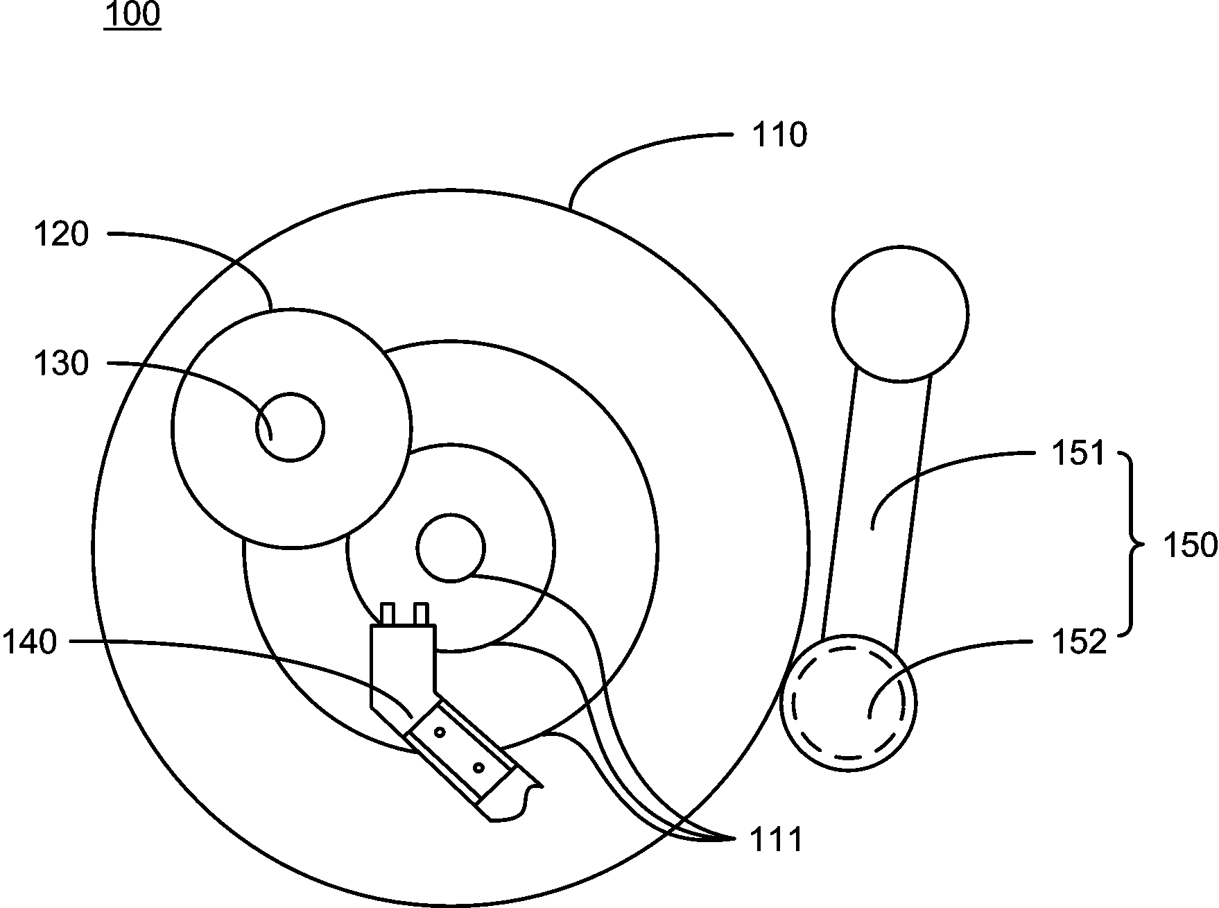
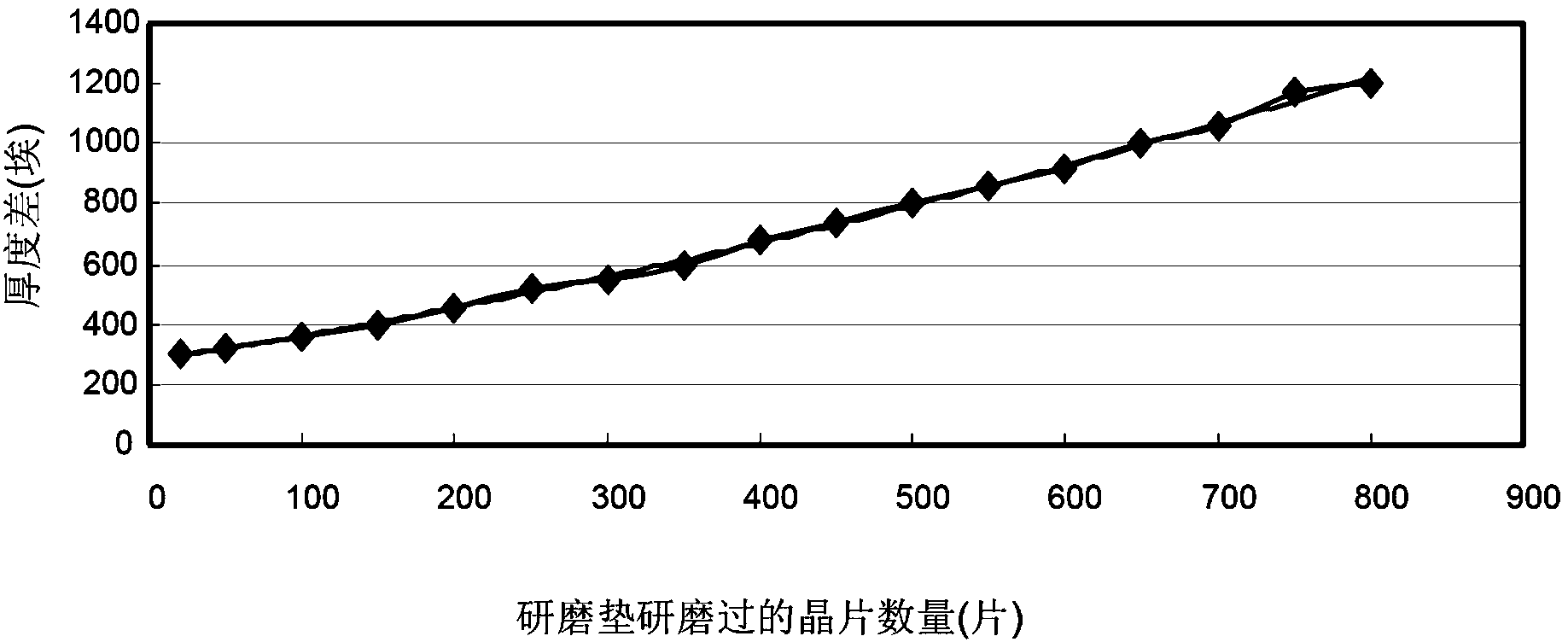
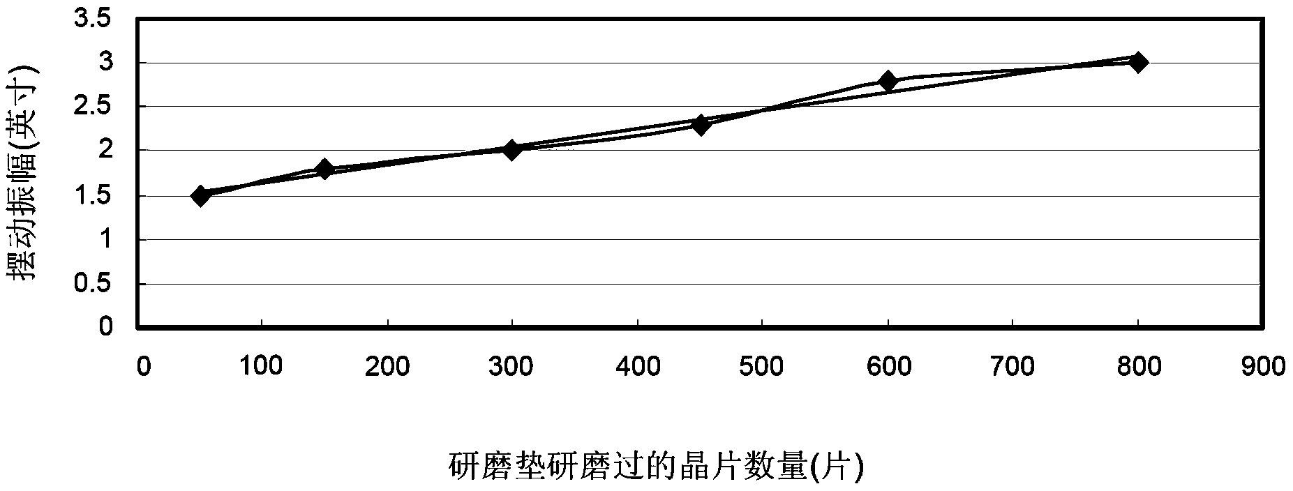
[0029] In the following description, numerous specific details are given in order to provide a more thorough understanding of the present invention. It will be apparent, however, to one skilled in the art that the present invention may be practiced without one or more of these details. In other examples, some technical features known in the art are not described in order to avoid confusion with the present invention.

[0030] In order to thoroughly understand the present invention, detailed steps will be provided in the following description, so as to illustrate how the present invention avoids the impact on the chemical mechanical polishing process with the prolongation of the use time of the polishing pad. Obviously, the practice of the invention is not limited to specific details familiar to those skilled in the semiconductor arts. Preferred embodiments of the present invention are described in detail below, however, the present invention may have other embodiments besides...


PUM


Abstract

The invention discloses a chemical-mechanical grinding system and grinding method for wafers. A layer of materials to be grinded is formed on the said wafers. The said method performs chemical-mechanical grinding on the said wafers by using an abrasion pad, wherein the said wafers sway along a radial direction of the abrasion pad by certain amplitude determined by a following method. The amplitude is determined by a first relation curve and the quantity of the wafers grinded by the abrasion pad; the said first relation curve is a curve showing a relation between amount of the wafers grinded by the abrasion pad and the said amplitude when the thickness difference between an upper edge area and a center area on grinded wafers reaches a target value. The Chemical-mechanical grinding method compensates the thickness difference between the center area and the upper edge area after grinding by adjusting the amplitude of the wafers' swaying along the radial direction of the abrasion pad in a grinding process, such that the appearance change of the wafers due to the long using time of the abrasion pad can be prevented.

Description

technical field [0001] The invention relates to a semiconductor device manufacturing process, in particular to a chemical mechanical grinding system and a method for grinding wafers using the system. Background technique [0002] With the development of semiconductor technology and the reduction of device size, photolithography technology has higher and higher requirements for the flatness of the wafer surface. Among them, chemical mechanical polishing (CMP) is a planarization method commonly used in the semiconductor manufacturing process. In addition, chemical mechanical polishing can also be used to remove films deposited on the wafer surface. The principle of chemical mechanical polishing includes the combination of chemical and mechanical effects. On the surface of the material layer to be polished, a specific layer is formed due to a chemical reaction, and then the specific layer is removed mechanically. [0003] figure 1 It is a top view of an existing chemical mech...

Claims


Application Information

Patent Timeline
Patent Type & Authority Patents(China)
IPC IPC(8): B24B37/07H01L21/02H01L21/3105
Inventor 邓武锋
Owner SEMICON MFG INT (SHANGHAI) CORP
Features
  • R&D
  • Intellectual Property
  • Life Sciences
  • Materials
  • Tech Scout
  • Unparalleled Data Quality
  • Higher Quality Content
  • 60% Fewer Hallucinations
Learn More